
|
PIC24FJ128 - Analog Digital Conversion
The role of the ANALOG-TO-DIGITAL CONVERTER (A/D) is to convert analog voltage values to digital values. Let’s explore the principle of operation of the A/D converter:
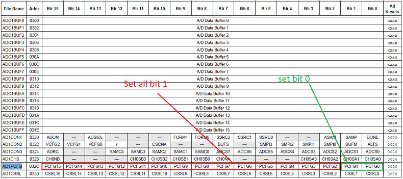
For this reason, the greater the bits, the greater the precision of the measurement. The PIC24FJ128 is a 16-bit microcontroller whereby a 5V density is separated by 16bit, so the PIC24 can read numbers after the decimal point. For this reason, during the conversion there are significant bits before the decimal point, and less significant bits after the decimal point Working Principle od ADC conversion on PIC24 From work register w3, I memorize in the register AD1PCFG from 15 to bit 2 as 1, and bit 1 and bit zero to 0 ( see register AD1PCFG). This means that I configure bit 0 and bit 1 as physically analogue input. mov #0Xfffc,W3 mov w3,AD1PCFG For more details see Figure 1 below
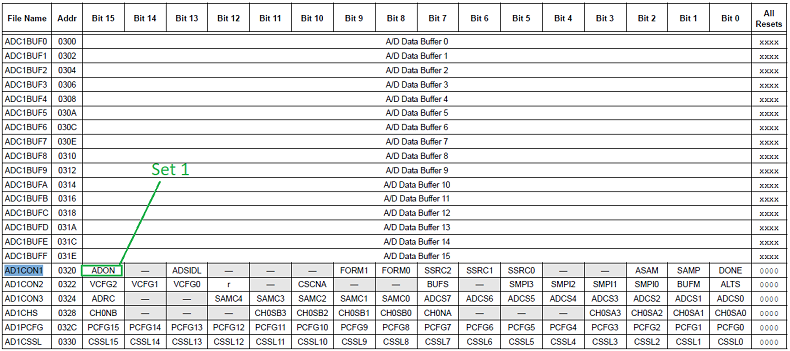
Figure 1 - AD1PCFG register Activate 1 the bit 15 (ADON) on the register AD1CON1 which represent the automatic conversion mov #0X80E0,W3 mov w3,AD1CON1 For more details see Figure 2 below
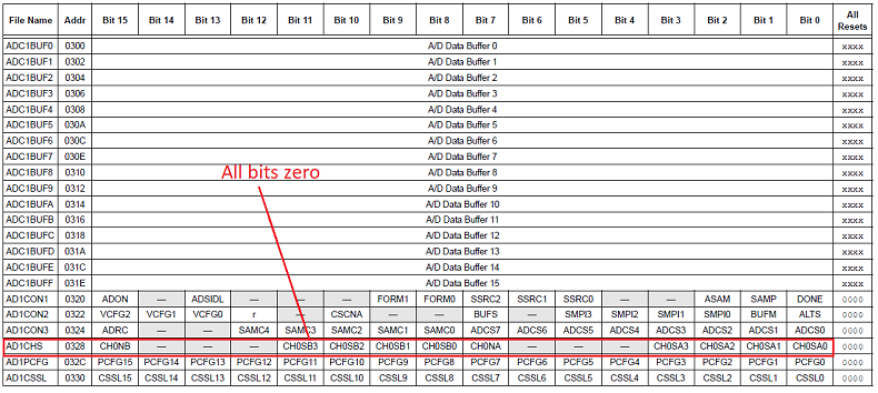
Figure 2 - AD1CON1 register I put all bits to zero in the register AD1CHS to enable the channel AN0 as positive (Channel 0 Positive Input Select for MUX A Multiplexor Setting bits) mov #0X0000,w3 For more details see Figure 3 and 4 below
Figure 3 - AD1CHS register
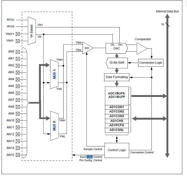
Figure 4 - 10-BIT HIGH-SPEED A/D CONVERTER BLOCK DIAGRAM
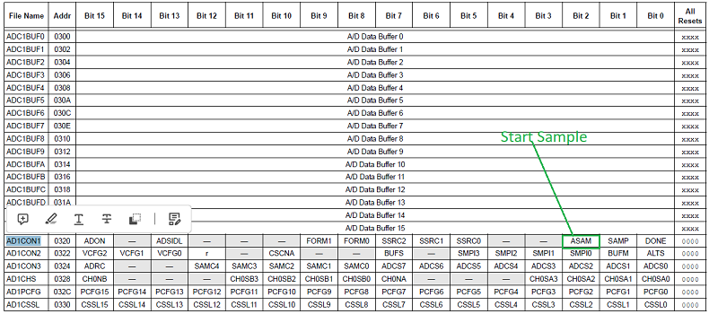
Start the sample by selecting bit 2 on register AD1CON1. Bits 5,6,7, was already selected previously 1, including also the bit 15. The bit 2 on register AD1CON1 when is 1 means the start of the sample mov #0X80e4,w3 mov w3,AD1CON1 For more details see Figure 5 below
Figure 5 - AD1CON bit 2 Start sample Next step is take sample from temporary register, in this case ADC1BUF0 mov ADC1BUF0,w14 This instruction moves the sample from the ADC1BUF0 register to the PORTD register to display the sample on the LEDs. mov #0X80e0,w3 Remove the start conversion, which means zero on bit 2 in the register AD1CON. The sample from Channel AN0 is completed and be ready for the next sample Next sample will be from chanel AN1 (analoque input) mov #0X01,w3 The instruction above shows that the sample will be taken from AN1 this time mov #0X80e4,w3 The instruction above is the start sampling (as previously) mov ADC1BUF0,w14 The instructions above show the new sample in the temporary register ADC1BUF0 and transferred to the PORTD for the Leds visualisation mov #0X80e0,w3 Remove start conversion after sampling completed Full routine of ADC conversion click here
|

+(39) 347 051 5328
Italy - Kazakhstan


09.00am to 18.00pm
About
We offer the best and economical solutions, backed by 27+ years of experience and international standards knowledge, echnological changes, and industrial systems.
Our Services
Marketing Materials


Marketing Materials1


