|
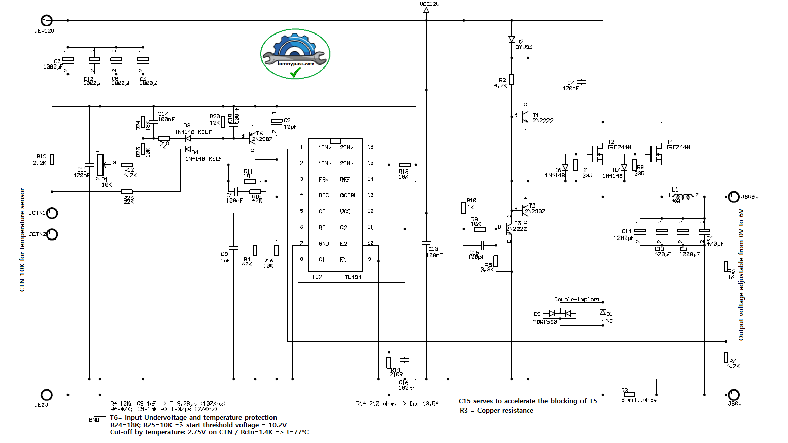
12V to 6V 10A DC DC Converter TL494
DC-DC Converter 2 pieces of IRFZ44N Coil 40UH 12V…14.4V power MOSFETs built on TL494 PWM control integrated converts the input voltage (12V) as 0-6V 10A. It has low voltage, short circuit and over-temperature protection.
This power supply is intended to power, from a 12V (lead-acid) battery, 6V motors mounted on a boat. It is equipped with a protection device in the event of:
- short circuit
- overheating of components
- input voltage too low
Features of TL494 DC-DC Converter Circuit
- Input voltage between 11v..14 volts
- Output voltage (adjustable with potentiometer) 0 volt 6 volt - 0A 10A output current
- Short circuit and overload protection (13.5A)
- Output current (10A / 6V) 90%
- Protection against overheating (CTN 10 Kohms) (75 °C)
- Cutoff frequency 37μs
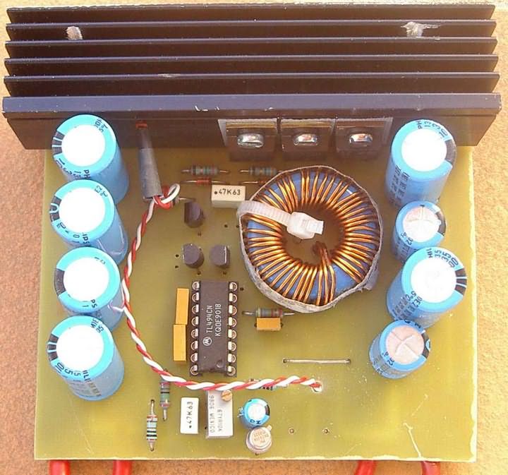
- Toroidal core properties used: – outer diameter = 28mm – inner diameter = 14mm – thickness = 9mm number of turns N = 16. – toroidal coefficient AL = 156nH (choking value for one turn) (L = AL * N2)
- To support maximum current, 2 wires of 0.8mm diameter each will be wound in parallel. The coil value thus obtained is 40μH.
- The R3 resistor used for current limitation is 0.008-ohm. The author provides this resistance via the PCB. Explanation: Current protection is achieved by measuring the voltage on the copper line. 75mm x 5mm = approximately 8 milliohms
- For short circuit current adjustment, you can change the value of this resistor or use trimpot instead of R25 resistor.
It is a switching power supply made around a specialized circuit (TL494) which will make it possible to create a voltage step-down. The power part is based on 2 transistors, a freewheeling diode and an inductor, all associated with a few filter capacitors.
The power transistors are MOS (IRFZ44N), N channel. The particularity of the assembly lies in the control of the Mos gates, this is achieved using a "Bootstrap" capacitor which makes it possible to apply a voltage equal to the input voltage (12V) between the gate and the source of the Mos to put them into conduction.
Warning: this has the effect of limiting the input voltage so as not to destroy the Mos transistors, I have not provided any particular protection at this level (the manufacturer announces 20V maximum between gate and source of the transistor). The maximum input voltage must not exceed 14V.
To improve the efficiency of the power supply, I chose a Schottky diode for the freewheel, but a fast diode BYW80-100 is also suitable, under these conditions, the efficiency is lower (-2%). A fast diode is essential for this assembly.
Power losses: they are distributed mainly over the Mos transistors and the freewheeling diode. They are therefore mounted on a dissipator to evacuate the calories. At the level of the Mos transistor we have 2 types of losses:
- Losses linked to switching times (ON and OFF) (not negligible at all)
- Losses linked to the resistance of the transistor in the ON position (17 milliohms announced by the manufacturer)
To reduce the parts of the type (2), you will need 2 transistors in parallel. In these conditions the speed limit can be too high, but it never becomes higher than the speed that can support the free wheel diode "D9", the MBR1560 diode supports 15A, which is where the current limit is set les mos supportent 35A chacun.
The switching frequency
The choice of this value is subject to several criteria:
- Reduce switching losses => reduce the switching frequency to reduce the number of switchings
- Limit the magnetic field in the choke to avoid saturation => reduce the value of the choke, but in this case we are obliged to increase the switching frequency to reduce the maximum current in the choke (di = dt * e/L ).
- Reduce the ripple of the output voltage and reduce the size of the components (capacitors and choke) => increase the switching frequency
- The switching frequency must be higher than an audible frequency (> 20Khz) to limit noise pollution.
Initially, I had planned a switching frequency of 100Khz (T=10µs), but I chose a frequency of 27Khz (period of 37µs) because I obtained a higher efficiency (+1%).
Current in the choke, output voltage ripple
There are 2 current modes:
- Discontinuous current mode, the current in the choke is canceled during the switching period.
- Direct current mode, the choke current never cancels.
For a choke of 40µH and a switching period of 37µs, the transition from discontinuous mode to continuous mode takes place for an output current of 1.5A
The current in the choke for Is > 1.5A is equal to Is+/-1.5A. The output voltage ripple is linked to this variation in current and filter capacitors. With a 3000µF filter capacitor, we obtain a peak-to-peak ripple of 40mV.
Maximum output voltage
For an output current of low value, we are in discontinuous current operating mode in the choke. This imposes a maximum output voltage to guarantee the correct operation of the control of the power transistor gates (in switching and not in linear). The conduction threshold voltage of these transistors is approximately 4V to 5V, the output voltage should therefore not be greater than (11-5) = 6 volts.
When the current is high enough, this problem disappears because we switch to permanent current operating mode in the choke. The freewheeling diode is conductive during the entire opening time of the Mos transistors, we thus find the value of the input voltage to control the gates of the Mos transistors.
The potentiometer allows you to adjust the output voltage from 0 to 6V, so you cannot exceed the upper limit of the output voltage.
Temperature, current and voltage protection
- Overheating protection: In the event of overheating of components mounted on the radiator, a CTN resistor limits the current, and blocks the power supply if necessary.
- Current limitation: Current protection is achieved by measuring voltage on a copper track (75mm x 5mm = approximately 8 milliohms)
- Input voltage too low: The input voltage must not be lower than a minimum value (11V) to guarantee the proper functioning of the control of the power transistors, for this purpose monitoring of the input voltage limits the current output if necessary, and blocks the power supply if the voltage is too low.
- Input voltage too high: There is no protection at this level! This voltage should not be greater than 14V.
TL494 6V 10A DC DC Converter circuit diagram
Components List
| Part |
Value |
Package |
|
Part |
Package |
Value |
| C1 |
100nF |
cms |
|
R1 |
33R |
|
| C2 |
10µF |
|
|
R2 |
4.7K |
|
| C3 |
1000µF |
|
|
R3 |
|
made on copper (8 milliohms) |
| C4 |
470µF |
|
|
R4 |
47K |
|
| C5 |
1000µF |
|
|
R5 |
3.3K |
CMS |
| C6 |
1000µF |
|
|
R6 |
1K |
|
| C7 |
470nF |
|
|
R7 |
4.7K |
CMS |
| C8 |
1000µF |
|
|
R8 |
33R |
|
| C9 |
1µF |
|
|
R9 |
10K |
CMS |
| C10 |
100nF |
|
|
R10 |
1K |
CMS |
| C11 |
470nF |
|
|
R11 |
1M |
CMS |
| C12 |
1000µF |
|
|
R12 |
4.7K |
CMS |
| C13 |
470µF |
|
|
R13 |
10K |
CMS |
| C14 |
1000µF |
|
|
R14 |
210R |
|
| C15 |
100pF |
cms |
|
R15 |
47K |
CMS |
| C16 |
100nF |
|
|
R16 |
10K |
CMS |
| C17 |
100nF |
cms |
|
R18 |
1K |
|
| C18 |
100nF |
cms |
|
R19 |
2.2K |
CMS |
| D1 |
not used |
|
|
R20 |
10K |
CMS |
| D2 |
BYV96 |
|
|
R24 |
18K |
CMS |
| D3 |
1N4148_MELF |
cms melf box |
|
R25 |
10K |
CMS |
| D4 |
1N4148_MELF |
cms melf box |
|
R26 |
22K |
CMS |
| D6 |
1N4148 |
|
|
T1 |
2N2222 |
|
| D7 |
1N4148 |
|
|
T2 |
IRFZ44N |
|
| D9 |
MBR1560 |
TO220 |
|
T3 |
2N2907 |
|
| IC2 |
|
|
|
T4 |
IRFZ44N |
|
| JCTN1 |
|
|
|
T5 |
2N2222 |
|
| JCTN2 |
|
|
|
T6 |
2N2907 |
|
| JE0V |
|
|
|
L1 |
40µH |
|
| JEP12V |
|
|
|
P1 |
10K |
TRIMMER |
| JS0V |
|
|
|
|
|
|
| JSP6V |
|
|
|
|
|
|
The choke used (L1) is made with a torus of:
- outer diameter = 28mm
- thickness = 9mm
- number of turns N = 16.
- coefficient of the torus AL = 156nH (value of the choke for one turn) (L=AL * N2)
I wound 3 wires together, each 0.8mm in diameter, to support the maximum current. The value of the choke thus obtained is 40μH.
For further information about PCB plates and other details, do not hesitate to contact us
|