
|
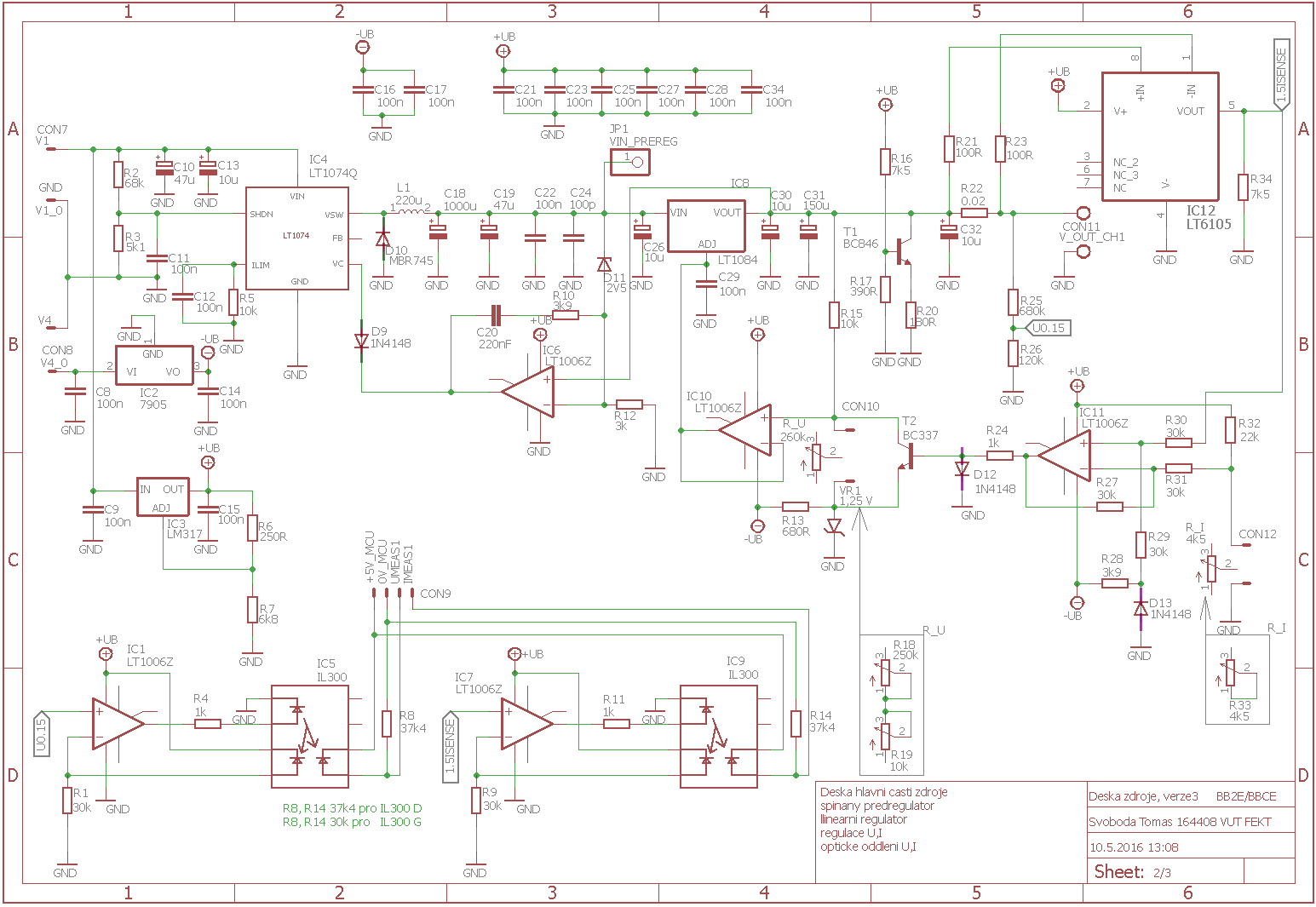
0-3A 0-30V Switching Digital Power Supply In the switching dc-dc digital power supply project with 0-30V voltage and 0-3A current adjustment, ATMEGA644 microcontroller was used in the control stage. The system is designed as dual ATMEGA644, which controls 2 power stages and displays voltage and current information on LCD screens. In the switching power supply driver power stages, LT1074 5 amp step-down dc-dc regulator integrated is used at the input, and then LT1084 5 amp adjustable dc-dc regulator integrated is used. The current is made by the LT6105 current sensing integrated circuit over a 0.02 ohm resistor, and voltage adjustments are made by the control stage with voltage divider resistors connected to the output. A toroidal transformer was used as the voltage source, 230v primary input and secondary outputs are 32V AC 3.2A 7V AC 0.1A 7V AC 0.3A. 0-3A 0-30V Power Supply MCU Power Solid Circuit Diagrams
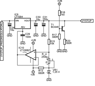
Design of the linear part of the power supply The linear stabilizer is based on the application of a classic three-terminal stabilizer. It can be used, because the power loss on it will be about 7 W in the worst case. The linear stabilizer used is LT1084, it is similar to the well-known LM317, but compared to it it has improved parameters and is designed for a higher current without the need for a booster transistor. The design is based on a basic circuit with an output resistive divider and a supply voltage of one polarity. In this connection, it is not possible to achieve a value of output voltage lower than 1.25 V, which is the value of its internal voltage reference. For more details see figure 3 below
Figure 3 - Connection of the linear part of the power supply Voltage regulation from zero can be achieved by connecting a sensing divider to a negative potential instead of a 0 V potential. For this case, a voltage reference of 1.25 V of the LT1004 circuit was chosen, which is suitable for this purpose. This reference is obtained from an auxiliary negative voltage source of -5 V. The resistance value of the resistor R13 can be determined from:
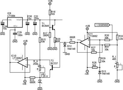
With the linear stabilizer used, it is necessary to ensure a minimum current consumption. Since the output voltage is regulated by a divider with a relatively large total resistance (see above), the need for minimum current consumption cannot be satisfied by this option. Failure to ensure the minimum current consumption was reflected in the simulation and practical implementation by increasing the voltage to the maximum value, which made it impossible to set the output voltage at the no-load capacity. A certain current consumption can be provided by a fixed output resistor, however, its value would have to be relatively small to ensure a minimum consumption for all output voltages and thus a relatively large power loss would arise on it. The consumption is determined by a simple current source, which consists of transistor T1, adjustment divider R16, R17 and emitter resistor R20. The base voltage is derived by means of a divider from the stabilized voltage value (the same voltage that is supplied to the OZ) and the value will be constant. Resistor R20, respectively. R17 can be adjusted to a given current. In our case, the value is about 5 mA. The current will vary in a relatively small range due to the output voltage, but the exact value of the current is not important for the application (within mA units). At a given current, a permissible power loss of approximately 130 mW occurs on the transistor. Auxiliary voltage sources The first auxiliary power supply consists of stabilization of the input voltage. Stabilization of this voltage has proven itself for the power supply of OZ, current sensing circuit and current source and optocouplers. Stabilization is carried out by the LM317 stabilizer, which is in the TO-92 case. The power loss on it, despite the higher consumption of optocouplers, is within the permissible limits. The calculation of the output divider for setting the output voltage can be done using the equation given in Chapter 1.7.4, the input and output capacitors are sufficient with a value of 100 nF (practically tested). An auxiliary negative voltage source is used for the possibility of regulating the voltage from the value Current limitation of the source Current limiting is a possibility to solve in several ways in general. In the case of a proposed resource, the following options can be used
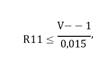
The first option would be the most reliable and least complex, but the switching stabilizer circuit (LT1074) has the ability to regulate current from about 1 A (given by the lowest possible DCL value of the circuit [15]. The second option cannot be used when a mere current limitation is required. The implementation of the fourth option is relatively simple and good features can be achieved, however, in terms of power dissipation, it is the least efficient option (the circuit practically behaves in a variable resistance on which power dissipation arises). The current limitation of the linear regulator itself is limited only by the design of the stabilizer and is fixed at a value of approximately 5 A.
Figure 4 - Current limiting circuit and its connection to a linear regulator Connecting the emitter of the transistor to a negative potential is necessary due to the limitation of the current from small current values, i.e. to achieve the possibility of a low (zero) output voltage. The base of the transistor is connected to the output of the operational amplifier, so the transistor is controlled by this OZ. To determine the value of the current through the load, the output of the circuit for measuring the current is used (the principle is described in more detail, among other things, in Chapter 2.11 below), which is also used for the current measurement itself. The op-amp works as a universal algebraic element with a transfer of 1 (provided by suitable resistor resistors R27,R29 – R31 = 30 kΩ). The operational amplifier must also have a negative power supply, due to the connection of the transistor emitter to a negative potential, otherwise the output voltage could not be limited to a value lower than 1.25 V). The non-inverting input IC9 (OZ) is supplied with a voltage directly proportional to the measured current (1.5· I) and a negative voltage obtained by a conventional diode (approximately 0.65 V). On the inverting one, the threshold voltage level set by the divider R27, R28 (R28 is a potentiometer). This connection has approximately the following function: UOUT, OZ = [(- 0.65) + 1.5· IZ]NEINV-[UR_I]INV where UOUT, OZ is the output voltage of the OZ that is applied at the base of the transistor, IZ is the current of the load and together with the coefficient of 1.5 forms the voltage applied to the non-inverting input and UR_I the voltage is applied to the inverting input, which is derived from the setting of the potentiometer to set the maximum current. The value of -0.65 is approximately the value of the voltage in V applied to the non-inverting input.
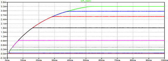
Figure 5 - Simulation of current limitation circuit
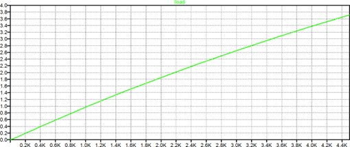
Figure 6 - Dependence of the maximum current on the setting of the potentiometer for current regulation
Voltage measurement The voltage measurement circuit consists of an input divider to reduce the measured voltage in a suitable ratio and an optical isolation, which is the subject of a separate chapter. The output of the measurement circuit is then connected to the A/D converter of the microcontroller, whose reference voltage will be 5 V. Voltage measurement will be in the range of 0 - 30 V. The reference voltage is obtained from the input stabilizer. Of course, this option is not suitable, as the output voltage will not be fully stable (fluctuating consumption due to the power supply of the relay coil, accuracy of setting, etc.), but practical testing has shown that this option does not affect the accuracy of measurements at a given resolution.
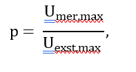
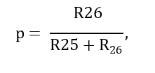
where p is the conversion ratio of the divider, Umer,max is the maximum considered voltage at the input of the A/D converter in V, and Uvyst,max is the maximum output voltage of the source in V. The conversion ratio itself for a resistive divider can be calculated as:
where R25 and R26 are the individual resistance values of the resistors in the divider in Ω.
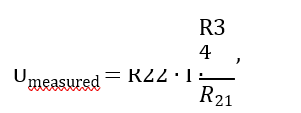
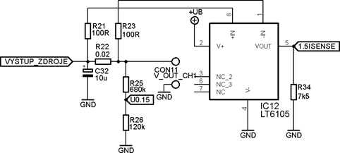
Current measurement The LT6105 circuit is used for current measurement, described in more detail in chapter 2.3.3. The wiring of this circuit is shown in Figure 2.13. The R22 resistor is sensing and is used with a value of 20 mΩ. Resistors R21 and R23 were chosen with a value of 100 Ω, they are the input resistors of the differential amplifier. An output resistor R34 should be designed. It is expedient that the output voltage is proportional to the current flowing through it with a conversion constant of 1.5. Thus, for a maximum load current of 3 A, the measured voltage will be 4.5 V. And for a minimum resolution of 10 mA, the relevant voltage measurement range will have a range of 15 mV – 4.5 V. The A/D converter used is the same as for voltage measurement and the resolution is therefore 5 mV. The resistance value of the output resistor can be calculated as:
After derivation and substitution, the output resistor value is 7.5 kΩ. The output voltage is again supplied to the A/D converter via a linear optocoupler. If the ratio of resistors R21, R23 (RIN) – R34 (ROUT) is inappropriately chosen, the output voltage will be non-linearly dependent on the measured current, which was found during the testing of the prototype.
Figure 7 - Wiring a circuit for measuring current
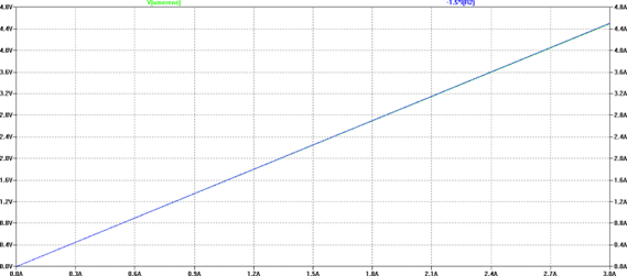
Figure 8 - Dependence of load current on current meter output voltage Figure 8 – the green curve is a simulated dependence of the output voltage of the circuit for measuring current versus current through a sensing resistor. This dependence is covered by a theoretical dependence of 1.5· I, which is the desired progression. The dependencies mostly overlap and it can be concluded that the output voltage corresponds to the measured current in a given ratio and in the entire area of the measured current. At a current of I=0 A, the output voltage is given by an offset of approximately 296 μV.
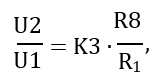
Optical separation Since the proposed power supply is designed as a two-channel power supply, it is required to be able to connect channels in order to obtain a symmetrical output of ±30 V against the ground, which must be separated between the individual channels. If the measured voltage was directly connected to the input of the A/D converter used, the ground would be connected. This problem is solved by using an isolation amplifier with optical separation. Optical isolation also protects the board with the auxiliary microcontroller in the case of high voltage at the output of the power supply and thus reduces damage, which is not the primary purpose in this application. The wiring with the IL300 circuit for isolation is shown in Figure 9, below. Resistor resistors R1, R8 can be proposed for from
where the constant K3 is defined by equation 2.1.
Figure 9 - Wiring the IL300 circuit to isolate the measured voltage
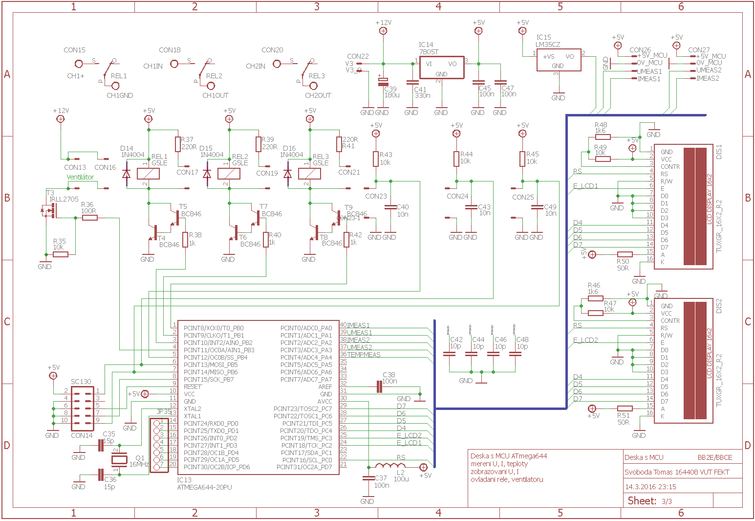
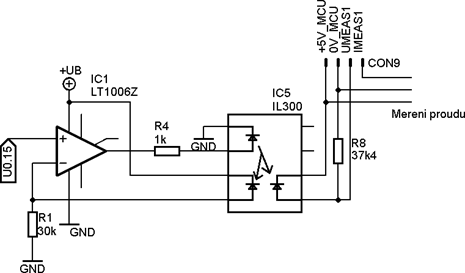
Microcontroller The microcontroller used is ATmega644, which will be used to measure voltage, current, display these values on the LCD, control the relay for connecting the output terminals and switch on the fan when the measured temperature is exceeded by an analog temperature sensor. The microcontroller can be programmed via the SPI bus in an already finished device, which is used here by the Atmel Ice programmer. Microcontroller Wiring The basic connection with the microcontroller is shown in Figure 10. The circuit is powered by a 5V 7805 stabilizer (not drawn). The CON14 connector is used to connect to the ISP programmer. The crystal is selected with a frequency of 16 MHz together with the recommended capacitor value according to. Pins 31-32 are used to connect an external reference voltage, since this option is not used, it is recommended to ground the AREF input through a capacitor. The L2 and C37 components form a simple low-pass filter. Power through this filter is required to power the analog part of the microcontroller. The components were selected according to [24]. Pins 1-7 are connected by buttons and transistors for switching relays (not drawn for simplicity). Pins 40-36 are used to measure voltage, current and temperature. Pins 25-29 are used to connect an LCD display that uses 4-bit communication. Capacitors C42, C44, C46, C48 help to reduce interference at the input of the A/D converter.
Figure 10 - Connecting the microcontroller to the circuit
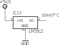
LCD Imaging The display is connected to the used MCU and is used to display the output voltage and current. A separate display will be used for each channel. It is a 16x2 display, i.e. a two-line display of sixteen characters per line. The display is equipped with a HD44780 controller (or equivalent), which simplifies communication with it. The basic connection with this display is shown in Figure 2.15, together with the microcontroller connection. Temperature sensing Temperature sensing is handled by a simple analog temperature sensor LM35. Its output voltage is directly proportional to the sensed temperature. The maximum temperature must not exceed 150 °C. The recommended wiring of this circuit [25] for sensing temperatures greater than 2 °C is shown in Figure 11
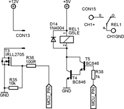
Figure 11 - Basic connection of the LM35 temperature sensor circuit The circuit in the basic connection does not require any external components. At the same time, great accuracy is not required from the circuit, so it is not necessary to use special wiring with this circuit to increase accuracy. Accuracy is not critical in this application – it will only be switching the fan when a certain temperature inside the device is reached, or disconnecting the output terminals of the power supply. The resulting voltage will be applied to the A/D converter of the used MCU and further evaluated. Relay and fan switching The relays are used for disconnecting inputs, switching the power supply and switching on the fan. The appropriate relays are switched by an NPN transistor, which is switched by an MCU. To guarantee correct switching, a Darlington connection of two NPN transistors is used, which achieves a higher amplification factor and a lower base current. A diagram of one such switch is shown in Figure 12 on the right. The base resistor limits the current of the base. The value is chosen so that not a large current is drawn from the MCU pin, and at the same time the necessary current is achieved relative to the current through the collector. The D14 diode is a protective diode that prevents the transistor from breaking down when the coil is opened. LED1 together with its resistor is used to indicate the status of the appropriate output of the source, in the end the option to display the status on the LCD was chosen and these LEDs are not fitted. The transistor must be selected with respect to the resistance of the coil and the supply voltage (current through the coil at the time of switching).
Figure 12 - Switching fan (left) and relay (right) from the MCU I must say that this is an excellent power supply, it has been built 18 times in our company. By making some changes it is possible to also increase its power and its automatic mechanisms. For more details do not hesitate to contact us |

+(39) 347 051 5328
Italy - Kazakhstan


09.00am to 18.00pm
About
We offer the best and economical solutions, backed by 27+ years of experience and international standards knowledge, echnological changes, and industrial systems.
Our Services
Marketing Materials


Marketing Materials1


