
|
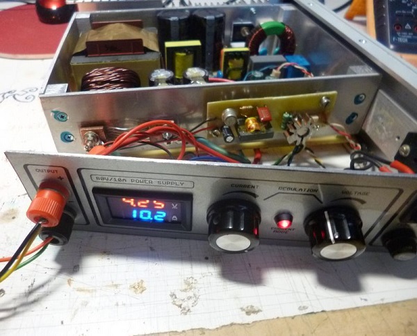
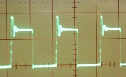
Adjustable SMPS Power Supply 0.2V-80V 0-10A TL494 0.2V-80V Switching power supply based on TL494 IC is used in various devices, motors, batteries, battery charging processes, etc. Designed for. There is an additional SMPS circuit with TNY267 integrated circuit to power elements such as TL494, Fan, Relay. Like many circuit elements used in the SMPS Project, this material was supplied from PC power supplies. Adjustable SMPS Circuit parameters: Input voltage: 210V – 265V, Power consumption and current: max. 860W / 4.5A, Output voltage: 0.2V-80V, Ripple: up to about 0.3V, Adjustable Output current: 0-10 Amp., Short circuit current limitation: 14 Amp.
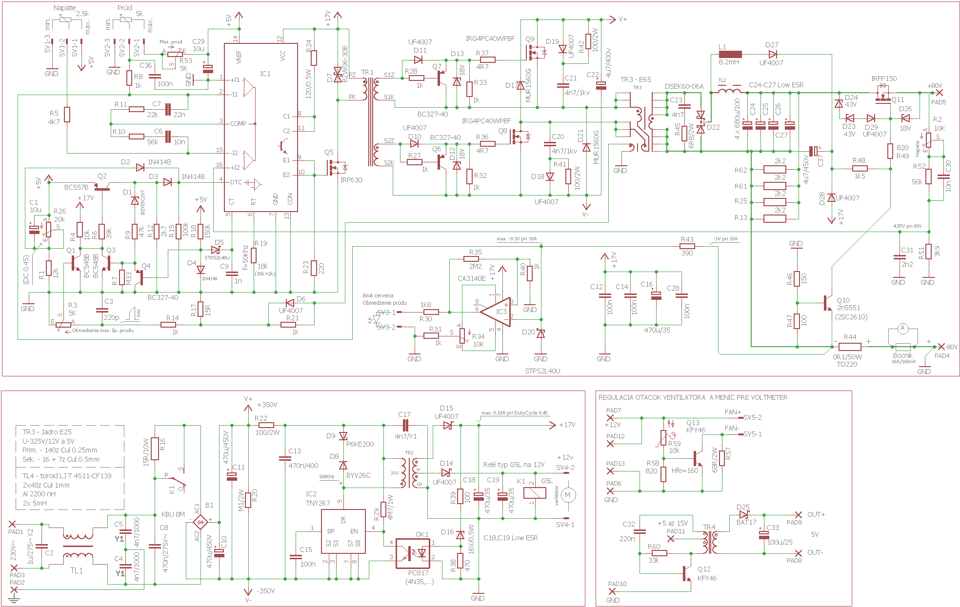
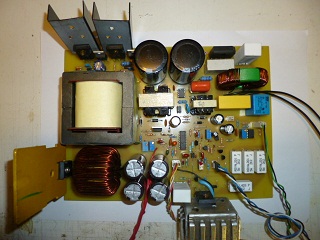
80V 10A SMPS Power Supply Circuit Diagram
Components List
Parameters
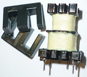
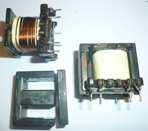
Feature The mains voltage passes through the input filter formed by the toroidal choke TL1 and capacitors C2, C8. The voltage is supplied to the bridge rectifier through the resistor R16 which limits the current surge caused by the charging of the smoothing capacitors after the power is turned on. After the start of the auxiliary source, relay K1 bridges resistor R16 and disables it from the circuit. Behind the rectifier, the voltage is filtered by a pair of electrolytic capacitors C10, C11. Both the main and auxiliary sources are powered by this voltage. Resistor R20 ensures the discharge of capacitors after switching off the source. The auxiliary source creates a supply voltage of 17V for the control circuit of the power source and 12V for the cooling fan. The basis of the auxiliary source is a proven integrated circuit from the TINYSWITCH-II family in a catalog connection. It is a blocking converter with a frequency of 132Khz and requires a minimum of external components. The supply voltage is supplied through resistor R22 and the primary winding of the transformer to pin 5 of IC2, which is the "Drain" of the switching transistor. The voltage is filtered by capacitor C13. Resistor R29 determines the starting threshold of the converter, the value of 4.7MΩ determines that the source starts to start when the input voltage reaches about 300V. Diodes D8, D9 protect the switching transistor from voltage peaks arising during the expansion of the inductive load. The damping element works as follows. When the transistor in IC5 is open and current flows through the primary winding, D8 is polarized in the closing direction and no current flows through the damping element. After opening the transistor, a voltage of the opposite polarity is induced on the primary winding, D8 is now biased in the forward direction and supplies a voltage to the cathode of transil D9. When the rising voltage reaches the opening threshold of the transil (200V), it opens and current starts flowing through the diodes. The voltage on the primary winding no longer increases. The damping element therefore limits the height of negative pulses to 200V. There must be an ultra-fast diode at position D8. C15 is a filter capacitor for the internal reference source. The secondary winding of the transformer has a 12V tap for powering relay K1 and for the cooling fan. The voltage from the secondary winding is rectified by the one-way rectifier D15 and filtered by the capacitor C18 (or D14, C19). Stabilization of the output voltage is realized by feedback through optocoupler OK1. Only the 17V branch of the source is stabilized. The twelve volt branch supplies only the fan and relay K1, therefore it does not need stabilization, its voltage is given by the transformer ratio. The stabilized voltage +17V is fed through the resistor R39 and the diode D16 to the LED diode of the optocoupler, if the voltage at the output reaches a voltage of 17V, the zener diode D16 opens and the current begins to flow through the LED diode in OK1. The diode lights up and partially opens the photo transistor which pulls the EN terminal of the control circuit to ground and blocks the pulses to the primary winding of transformer TR2. The moment the voltage drops, the pulses are restored. The value of the output voltage of the source 17V was chosen with regard to the control voltage of the IGBT transistors, at this voltage the transistors are already safely open. Main source As the control circuit of the main source, the integrated circuit TL494 is used in single-action mode. I chose this circuit because it has two separate control amplifiers and the voltage at their inputs can vary from -0.4V to the supply voltage. It is therefore possible to regulate from scratch. Single-acting / double-acting mode is switched by connecting pin 13 of IC1 to ground or +5V. By connecting to ground, the circuit works as a single-acting source. The frequency of the sawtooth generator is determined by the capacity of the timing capacitor C9 and the resistance of the resistor R19. The frequency is set to 50Khz, calculated according to the formula [f = 1/(R*C)]. The output transistor in IC1 and transistor Q5 together form the driver of the decoupling transformer. The bidirectional transil D7 protects the power transistor from voltage peaks arising during the expansion of the inductive load. Transistor Q5 can be of type IRF540, IRF630, etc. A wound power transformer from a 350W PC source is used as the excitation transformer. I will give the winding prescription and details at the end of the article. The transformer is wound as permeable and the sense of the windings must be respected. When the transistor Q5 is open, a positive pulse is generated on the secondary windings of the transformer, which charges the gate capacity of the IGBT transistor Q9 through the diode D11 and the resistor R37. Resistor R37 limits max. peak current when charging the gate. R33 forms the minimum load of the excitation transformer TR1 and helps discharge the gate of the power transistor Q9. Zener diode D13 protects the gate against exceeding the maximum allowed voltage, which is usually 20V. Transistor Q7 is closed during the positive period, because due to the voltage drop on diode D11 (about 0.7V), the voltage at the base of the transistor is more positive than at the emitter. After the end of the excitation pulse, the energy accumulated in the magnetic field of the transformer core tries to maintain the direction of the current and the polarity of the voltage on the secondary windings is reversed. A negative signal period occurs. The charge accumulated on the gate capacitance of the power transistor Q9 maintains a positive voltage on the emitter of the transistor Q7. Diode D11 is now reverse biased and closed. The current from the excitation transformer now flows through resistor R28 to the base of Q7, which opens and avalanche discharges the charge accumulated on the gate capacitance of transistor Q9. Transistor Q9 closes. The above also applies to the driver of the second power transistor Q8. Power transistors Q8, Q9 and diodes D17, D21 form the final stage for driving the power transformer. The transistors must be fast IGBTs with a current of around 30A. The topology of the exciter with switching of both ends of the winding is chosen for the following reasons. A power transformer is sufficient with only two simple windings. Power transistors are not threatened by high voltage and cheaper types are sufficient. The function of the final stage is as follows. Both transistors Q8,Q9 are opened at the same time. The excitation current flows from the positive terminal of the filter capacitor through transistor Q9, the primary winding of the power transformer and transistor Q8 to the negative pole of the filter capacitor. The impulse current reaches up to 37 amperes. Through the passage of current, part of the energy accumulates in the magnetic field of the transformer and part flows to the secondary side. After the end of the excitation pulse, transistors Q8, Q9 are closed. The accumulated energy in the core tries to maintain the direction of the current in the windings, part of the energy still flows through the secondary winding and part is induced back into the primary winding but with the opposite polarity. Since the return voltage is of the opposite polarity, the recovery diodes D17, D21 open and connect the winding in the correct polarity to the filter capacitor. The passing current back-charges the capacitors, returning part of the energy back to the input. This increases the efficiency of the source and effectively limits the voltage peak to the size of the voltage on the filter capacitors. Additional RDC cells protect the power transistors against too fast voltage rise on the "drains" when the load is switched off (dU/dT). Diodes D18 and D19 must be ultra-fast with a breakdown voltage of at least 800V. The RDC cells must be placed as close as possible to the terminals of the transistors. Capacitor C22 covers current peaks arising when switching transistor Q8 because it is located further from the filter capacitors. At first glance, the TR3 transformer is drawn strangely, but it is not a special part. It is a simple transformer with two windings, just to the end of the winding, between the body and the pins of the body, a toroidal ring of the current transformer is strung for measuring the peak current of the power transistors. The secondary winding of the current transformer is connected to the two outermost pins of the power transformer. From the point of view of the printed circuit board, both transformers form one component. The goal of this solution was to reduce the parasitic inductances of the transformer terminals and to simplify the circuit board. The power transformer is followed by a one-way rectifier formed by the upper half of the D22 diode. In the active period of the signal, when the positive polarity of the voltage at the upper end of the secondary winding, the upper half of the diode D22 is biased in the forward direction. The diode is open and current flows through it, which continues to flow through choke TL2 and charges smoothing capacitors C24, C25, C26, C27. Capacitors must have low series resistance (Low ESR). At the same time, the energy is stored in the choke TL2. In the inactive period, the upper half of D7 is closed, and the energy accumulated in TL2 is supplied to the load through the lower half of the diode D22. From the output filter, the voltage is already supplied through transistor Q11 to the output terminals of the source. The feedback control voltage is taken from the output of the source, through the resistor divider R2, R52, R51, R13. With an output voltage of 80V, there will be a voltage of about 4.75V at the non-inverting input, pin 16 of IC1. The voltage from the potentiometer for adjusting the voltage is applied to the inverting input of the control amplifier. By changing the pulse width, the control loop tries to match the output voltage and thus the voltage at the non-inverting input so that the voltage difference at the inputs of the control amplifier is zero. The output voltage is measured only at the terminals of the source in order to compensate for all voltage drops that occur in the circuit. (decrease in resistance Q11, wire resistances, printed circuit resistance, etc.) Fineness of voltage regulation depends on the quality of the potentiometer, so I recommend using a higher-quality sealed, linear potentiometer with a larger diameter. Preferably double 5KΩ and connect both sections in parallel. The gain of the bias voltage amplifier is determined by the RC element C6, R10. Too high a gain results in oscillation of the source. The soft start of the source and the protection of power transistors against current overload are implemented by transistors Q1 to Q4 and several components around them. The principle description from the manufacturer is in the document "Designing Switching Voltage Regulators With the TL494". Both functions affect the width of the excitation pulse, using the DTC input pin 4 of IC1. The voltage at this input can range from 0 to 5V, while at about 3.3V the pulse width is 0% and at 0.1V it is 90%. The maximum pulse width is set by resistor divider R1, R26, in our case 45%. Components C1, R26, R1, D2 ensure a soft start of the source. After switching on the power supply, capacitor C1 is discharged and 5V voltage from the reference voltage source is supplied to the DTC input via diode D2. By passing the current through the resistor R26, the capacitor C1 starts charging. The voltage on the DTC starts to drop, the pulses gradually expand up to the value set by the divider R1, R26. A short circuit at the output of such powerful sources is a serious matter, especially at the highest voltage, when the smoothing capacitors are fully charged. It melts the supply cables, creates an arc, splashes molten metal and there is a risk of injury to the operator as well as damage to the source. Therefore, the output of the source is protected against excessive short-circuit current. This protection ensures that in the event of a short circuit at the output, a current greater than 14A will not flow through the output terminals. The foundation is formed by transistor Q11, which is connected in series with the positive branch of the source. The transistor is held in the permanently open state under normal operating conditions by the +18V voltage supplied by resistors R48 and R49 to the control electrode of Q11. Since its on-state resistance is only 8mΩ, the voltage drop is negligible. Operating current can flow through the transistor without being limited and the transistor does not even heat up. When the output terminals are short-circuited, current will flow through resistor R44 and a voltage drop will occur. Transistor Q10 is biased against resistor R44 so that R44 acts as a positive voltage source for the base of transistor Q10. The base is connected through a 1:2.5 divider formed by resistors R46 and R47. When the voltage on the resistor R44 reaches about 1.4V (at a current of 14A), the transistor Q10 opens and the gate of the transistor Q11 is discharged through R49, it closes and the flowing current decreases. As long as the short-circuit current persists, transistor Q11 maintains the current flowing at 14A. Since resistor R44 is common to both short-circuit protection and current limiting, the excitation pulses to the terminal transistors will be blocked for the duration of the short-circuit current and the source will be shut down. Choke L1 and diode D7 form a voltage source for the "floating" transistor Q11. The voltage on the Q11 gate must always be +18V higher than the output voltage of the source. If the output voltage is below 17V, the voltage on the capacitor C37 is too low and the gate Q11 is powered through the diode D28 from the auxiliary source. When the output voltage of the source is above 17V, the voltage on C37 will increase so much that the diode D28 closes and the gate is powered via L1 and D27. The voltage on C37 can reach up to 150V at full power of the source, transistor Q10 must also be sized for this voltage. Diode D26 protects gate Q11 from exceeding the permitted voltage. Diodes D23, D24, D29 protect transistor Q11 against exceeding the maximum collector voltage. The next and last part of the source is the resistive load. This is mainly needed to speed up the source's response to control changes. Without a load, when the voltage potentiometer is quickly turned from maximum to minimum, the voltage would only drop very slowly. With load, the source reacts to changes in the control elements faster. It also realizes the minimum resource load. At low consumption, it still switches to intermittent mode, which is manifested by a weak hum coming from the transformer. The source must not whistle, if it whistles something is wrong. Construction and revival I originally designed the wiring without trimmers using only fixed resistors. Compiling the required resistance value proved to be very difficult, time-consuming and inaccurate. That's why I ended up using precision, multi-turn trimmers. I recommend using them even if they are a bit more expensive. The voltage potentiometer is a double linear 2x5k, sections connected in parallel. The current sensing resistor R44 must be of good quality, preferably in a TO220 case. An ordinary wire resistor cannot be used because the ceramic in which it is embedded is not capable of dissipating the generated heat. The stability of the current limitation is directly dependent on the stability of the resistance under changing temperature. When I used a regular ceramic resistor and set the current limit to 10A, after a few minutes the current started to drop as the temperature of the resistor rose. After ten minutes, the source was already delivering only 6A. Wires to terminals and potentiometers should be used as short as possible. The cross-section of the wires to the output terminals should be at least 4mm², so that the voltage drop is as low as possible. This needs to be fulfilled especially if we want the source to deliver a current of 10A to the load starting from 1V at the output. Potentiometers should be used preferably sealed or at least somehow protected against dust. Mains fuse around 6 to 8A. I make labels by printing the template with a laser printer in mirror image on a transparent film and pasting it with self-adhesive wallpaper of the desired color. I stick the label on the front panel with thin double-sided adhesive tape. I will leave possible modifications and improvements to the reader. Preparation the Winding Parts In order not to get entangled in winding directions, the good old lesson still applies: "twice a change is not a change". This means that if we flip the ends of the windings, we must wind all the windings in the same direction. Conversely, if we wind the individual windings in the opposite direction, then we must no longer swap the ends. The dots at the ends of the windings in the wiring diagram indicate the sense of the windings, while on the circuit board they indicate the actual beginnings of the windings. Therefore, we wind all transformer windings Tr1, Tr2, Tr3 in the same direction, and the dot tells us where to connect the beginning of the wire.
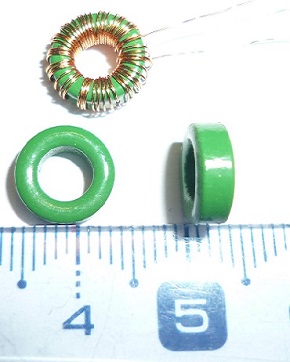
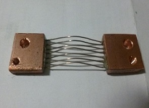
Table 1 - Construction of the measuring current transformer
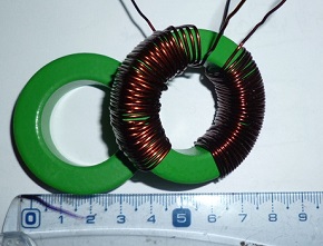
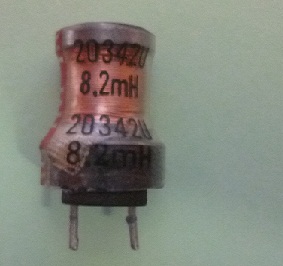
Table 2 - Construction of the suppression choke 2x5mH, input network filter
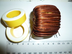
Table 3 - Choke L1 for supplying protection against excessive short-circuit current
Table 4 - Ammeter shunt
Table 5 - Power transformer design
Table 6 - Construction of smoothing choke TL2
Table 7 - Construction of transformer TR2
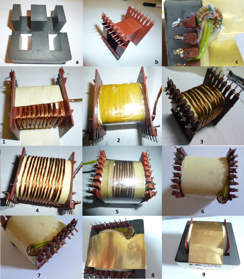
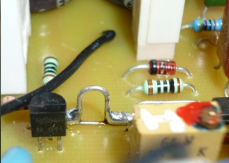
Table 8 - Construction of excitation transformer TR1 once we have finished all the winding parts, we need to collect the other parts and check the cases, or modify the design of the printed circuit board and make the printed circuit board. First we install the small parts, then the big ones and finally the transformers. We are not installing the TR3 transformer yet. We solder wire eyes to the marked jumpers. We will create measurement points as in the image to the right. We will connect potentiometers, LED current indicators, or an instrument meter for voltage and current. Turn the voltage potentiometer to the left to the minimum and the current potentiometer to about 10%. We will put some coolers on the transistors, small ones are enough, the transistors don't get particularly hot. Green hatched areas, "hacesoft" layer, need to be roughly tinned. For more details see Figure below
WARNING! In no case do not connect the source to the network without going through the recovery procedure! Without TR3
The owner of the updated project, @Niki31, commented on important edits. The translation is below. Thanks @Niki31 This power supply is very robust, it has been built 10 times. His results are excellent. All electronic components including the PCB plate, are available here on the site. For further details do not hesitate to contact us. |

+(39) 347 051 5328
Italy - Kazakhstan


09.00am to 18.00pm
About
We offer the best and economical solutions, backed by 27+ years of experience and international standards knowledge, echnological changes, and industrial systems.
Our Services
Marketing Materials


Marketing Materials1


