|
ADC STM32 ISSUE on STM32F100C8T6BB
Having mastered STM32 a little, I began to get acquainted with the ADC. A lot of information is contained in document AN2834. But there are useful recommendations, as on page. 37: Do not add any external capacitor (Cext) to the input pin when applying this above workaround alternate with harmful advice, as on page. 39: An extra large Cext enables sampling more often. This prompted the post to write (updated).
Modern ADCs, as a rule, have in their composition UVH. Moreover, this UVC is connected directly to the input pin without any buffers, because with unipolar nutrition, making a buffer problematic. In some Sigma delta ADC there is such a buffer, but it is usually disconnected, since restrictions on the permissible range of input voltage are imposed when using it. There is no input buffer in the STM32. During the sample to the input pin, the UVH capacitor is connected through the key. But what happens to this capacitor next? By the time of the next sample, will it be the previous charge? I don't think so. The fact is that modern integrated ADCs of this class are built on the basis of a capacitive DAC. During the conversion by the sequential approximation method, charges are balancing (rather than currents, as was the case in the ADC based on the R-2R CAPS). Therefore, the charge of the input capacitor is spent during the conversion. And in general, in many ADC capacitor UVH is not some separate element, but the entire matrix of capacitive DAC capacitive. So what will happen to the capacitor at the end of the conversion, it will run out to zero, or will it be charged with some other charge? It depends on the specific ADC scheme. Documentation does not give a clear answer to this question, you will have to resort to measurements.
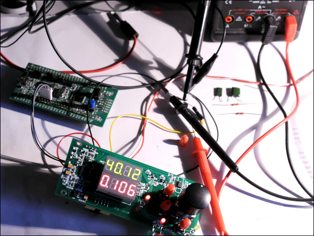
Consistently with the input of the ADC, I turned on the resistor 10 kOhm, the voltage drop on which was controlled by the oscilloscope. On all oscillograms horizontally 2 mks/del, vertically 100 mV/s. ADC works with a sampling frequency of 100 kHz. The measurements, of course, are not entirely reliable in terms of the form of the ejection, since I connected a small additional capacity to the ADC input (the 1:10 probate has a capacity of about 18 pphs). But the picture does not change qualitatively.
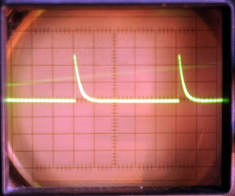
With zero input voltage, we see up throws. This means that a load-charged capacitor is connected to the input, which is discharged through the signal source during the sample. We have the resulting input current.
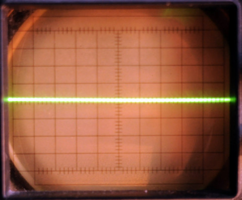
With a voltage equal to half the scale, emissions disappear.
At maximum input voltage, the emissions changed the sign. Now during the sample, the capacitor is charged from the signal source, we have a flowing input current.
In order not to appear an error of measurement, during the sample, the UVH capacitor must have time to charge to the input voltage with an accuracy of not worse than 1 LSB. It is easy to get this, since the capacitor capacity is small, about 8 p. The datasheet contains the corresponding plate, the
resistance value at the ADC input can be about dozens of kOhm. For sources of signal with high input resistance, you can increase the sample time of ADC, in STM32 there is such an opportunity.
But what will happen if the ADC on the container to the ground is turned on from the ADC entrance? This is a typical technique recommended almost everywhere. Together with the input resistor, this capacitor forms an anti-alias filter, which is always necessary, plus a filter from interference is obtained. If the capacity is turned on at the inlet of the ADC, the voltage emissions are razmased in time and by the end of the sample the voltage may not have time to reach the input with 1 LSB accuracy. We'll have to increase the sample time so that everything will fall into place. But this is possible for small tanks of about dozens of p. However, we usually talk about containers of about 10 x 100 nF. No increase in sample time will help. At the inlet of the ADC emissions will disappear, we will see some average voltage value. But that value is not equal to the measured stress. With an increase in capacity, the ADC error tends to its theoretical maximum. Although it would seem, what can be the damage from the tank at the ADC input, except for narrowing the band of the signal?
Let's check in practice. At the inlet of the ADC, the same 10 kOm, the ADC 4001 readings that correspond to the specified input voltage. Connect to the ADC input capacity 10 nF. The testimonies were 3987, i.e. ADC began to lie 14 units down. Now we reduce the input voltage. ADC indications without capacity 101. Connect 10 nF. The testimonies were 116, i.e. ADC began to lie 15 units upwards. The board to include the container at the entrance of the ADC is harmful.
The effects are easily calculated by operating the average ADC input current. This current is easy to measure, the double-integration ADC tester will show exactly the average input current. At zero input voltage, the current was equal to -1.13 uA, in the middle of the scale it is zero, at the maximum input voltage it is +1.09 mAh. That is well consistent with the calculations. According to datasheet UVH capacitor has a capacity of 8 pF. It is recharged on a maximum of 1/2 scale, which at a support voltage of 3.3 V is 1.65 V. The charge will be equal to Q - V * C. And the average current at the sampling frequency Fs will be equal to Iavg - V * C * Fs * 1.65 * 8E-12 * 1E5 * 1.32 uA. This almost coincides with the measured value. The input current is proportional to the sampling frequency, the measurement at zero input voltage and the frequency of 50 kHz gave a value of -0.56 uA, which also corresponds to the theory.
It would seem, well, well, the error that appeared can be taken into account when calibrating. At the same time, it should be remembered that the frequency of ADC samples should be constant, otherwise such calibration will be incorrect. But here's another problem. ADC is multi-channel, so the capacity with some charge obtained after conversion in one channel is connected to the input of another channel. The mutual influence of the channels. On the oscillograms below, the input of the ADC channel 1 with two channels running. The middle input current of the channel is also provided
ADC1 - 0, ADC2 - 4000. Iavg(ADC1) -2.45 uA.
ADC1 - 0, ADC2 - 2048. Iavg(ADC1) -1.64 uA.
ADC1 - 4000, ADC2 - 2048. Iavg(ACP1) ? +1.99 uA.
ADC1 - 4000, ADC2 - 0. Iavg(ACP1) ? +2.51 uA.
As you can see, the voltage at the input of channel 2 directly affects the input current of the channel 1. And this current can be twice as high as when one channel is running. This is also affected by the readings, if the RC chain enters, the readings of the channel 1 changed when the voltage at the input of the channel 2, the error reached 30 units. For the worst case, the answer to the question "what happens with the UVH capacitor happens later" can be given in this way: during each sample, the UVH capacitor must be recharged by the size of Vref. The average ADC input current for the worst case should be taken by Iavg Vref * South * Fs.
Conclusions - the first case: in order to have the right to connect a large-capacity capacitator to the ADC inlet, the resistor at the inlet of the ADC (along with the internal resistance of the signal source) should not exceed such a value when the average input current creates a voltage drop on it no more than 1/2 LSB. I mean, I.e. R - 1 / (2 ?(N+1) * Suvh * Fs), where N is the bit size of the ADC, the carc bush is the capacity of the internal UVH, Fs - the sampling frequency. For the built-in ADC STM32 and Fs 100 kHz, the resistance must be no more than 153 ohms. When the sampling frequency decreases, the resistance can be increased proportionally. The sample time in this case does not affect.
Conclusions - the second case: if for some reason the resistor can not be so small (for example, if the signal source itself has a higher output resistance), then an arbitrary capacity cannot be connected to the ADC input. If the capacity exceeds some value, an error will appear, which, with the capacity increase, will reach its maximum, as mentioned above. The question arises which denomination of the container is permissible for the selected resistor. The lower the sample rate and the more sample time, the more the capacity can be. You can probably make a formula, but I instead made a model of the input part of the ADC. In addition to the external RC chain, the internal capacity of UVX and the resistance of the key are taken into account.
For the frequency of samples of Fs 100 kHz and the sample time of 2 microns to obtain an error of no more than 1/2 LSB when resisting the resistor 100 ohm, the capacity shall not exceed 10 nF, and when resisting 1 kOhm, the capacity shall be no more than 330 pF.
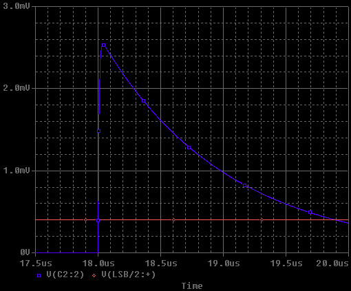
The following chart is removed for 1 kOhm resistor and capacity 4.7 nF. It is clear that the voltage at the input of the ADC never reaches the input, so there will be an error. With an even greater increase in the pulsation capacity at the inlet, the ADC decreases, but these pulsations do not occur around the input measured voltage, but around some average ADC input voltage, which differs from the measured voltage by the magnitude of the fall at the input resistor.
In order not to resort to modeling, RC-chain denominations can be calculated using simplified empirical formulas. In [1] it is recommended to choose an external capacity of about 20 times the capacity of UVX. The resistor is selected for reasons of the time of determination of the voltage on the container with an accuracy of 1/2 LSB. In this case, you can enter a certain coefficient k, which for the selected bit of ADC shows how many times the chain time should be less than the sample time. For 10 bits k ? 8, for 12 bits k ? 9, for 14 bits k? 11, for 16 bits k ? 12. I must say that the values of this coefficient are approximate, since the ratio of the external container to the capacity of the UVH is not taken into account. But these values can be used, taking a constant time with some reserve less than the estimated. For the above example, the calculation for 12 bits, the picking is 2 microns, C to 330 pF gives R approximately 700 Ohm. According to the results of modeling R - 1000 Ohm. A good match.
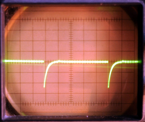
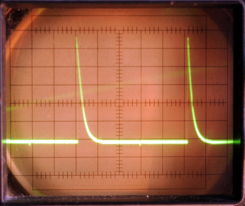
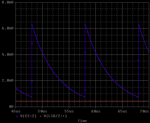
There is another function of the RC chain at the inlet of the ADC. It isolates the exit of the buffer OU from the ADC entry and prevents parasitic fluctuations. If the source of the signal is OU, then with a sharp change in the load current (which happens at the time of the start of the sample) at its release, an attenuating oscrow process may begin. In this case, in small times, the sample can get an unpredictable amount of error. Here is how the built-in buffer OJU of the DAC STM32, loaded at the input of the ADC through the resistor 100 ohm (scale - 100 mv/decade and 1 mc/s).

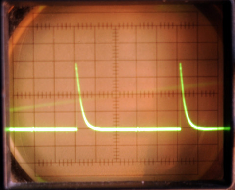
visible attenuating fluctuations, which last almost 2 mx. The increase in the resistor to 1 kOhm increases the emission at the inlet of the ADC and shortens the oscillating process a little. But it does not completely eliminate:

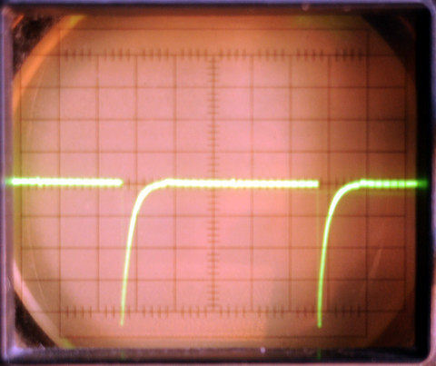
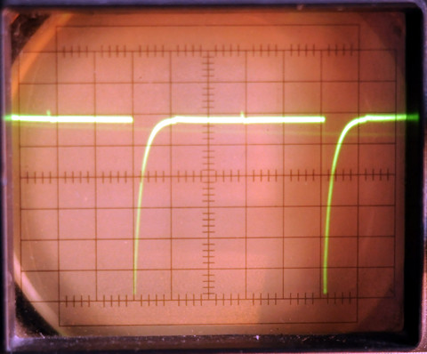
When connected after a resistor 1 kOhm, even a small capacity, such as 100 pF, the fluctuations disappear:
Therefore, the advice "Do not add any external capacitor" can also not be attributed to useful. In datasheets, most similar ADCs are recommended to include an RC chain at the input. The main thing is to choose the right denominations. It should be noted that by connecting the RC-chain to the OC output, you need to make sure that the OU is stable when working on such a load. Different types of OUs have different ability to work on a capacitive load, the determining parameter here is the output resistance of OU with an open loop of the OS. Usually, the relevant data is available in datasheet on the OU.
The above choice of the tank "twice as many as the capacity of UVX" is largely arbitrary, no physical meaning this coefficient does not carry. The external capacity is often called a "charge reservoir" for the UH tank. Ideally, the size of this capacity should be such that when charging the capacity of UVC, the voltage on it falls no more than 1/2 LSB. I mean, I.e. the size of the external tank for the 12-bit ADC should be more than the capacity of UVH in 8192 times. The corresponding R denomination will be very small, real OU is unlikely to be able to work on such a load. Therefore, a less stringent criterion for choosing a container is used. Then part of the charge receives the capacity of UVH from the external capacity, and part - due to the output current of the U.S.
If the ADC is used to digitize the alternating voltage, then it should also be noted that the resistance on the input affects the level of distortions due to the dependence of the ADC input current on voltage. The scorations begin to rise with an increase in the denomination of the resistor above the critical value mentioned above. The nature of distortions is the same as the nature of a static error in the measurement of constant stress.
And one more aspect: if the analog signal that arrives at the input of the ADC is used for something else, then the ADC entry can be an additional source of interference - "needle" with a sample rate. The best option is to unleash the ADC input from the rest of the analog circuit with a separate buffer on the OU. Then the necessary filtering can be performed at the inlet of the buffer, without limiting itself to the limits of the permissible resistance at the input.
Sometimes oversampling are used to improve the effective estrough content of ADC. In this case, the sample frequency is selected more, which entails an increase in the average input current. In addition, in the calculations you need to take an error 1/2 LSB not for the original ADC, but for the output code of increased bit size. This will further limit the values of R and C on top.
When increasing the effective discharge by adding a triangular signal to the input of the ADC (similar to Figure 22 of the document AN2834), the denominations must be selected taking into account the average input current of the ADC. If a capacitive divider with a relatively large capacity from the ADC entrance to the ground is used in such a scheme, the input resistor shall be selected small as described for the first case.
Below are a few links to the documents where such issues are discussed. It should be noted that nowhere is the moment concerning the error associated with the average input current of the ADC is not considered. This is probably due to the fact that they usually consider external ADCs, and there the constant time of the input RC chains are chosen small, so as not to lose the ADC input signal. In cases where slow signals are required, a slower ADC is chosen, it will have less than the average input current at the expense of a lower sample rate. The peculiarity of the built-in ADC is that we do not choose it. It, having a fairly high speed, can be used to digitize slow signals. In this case, it is easy to face a situation where the RC circuit does not yet limit the range of the useful signal, but already leads to an error on the DC. The average input current is sometimes considered when describing the ADC sigma delta, for them the digitization of slower signals than the ADC itself is a typical situation.
- Optimize Your SAR ADC Design
- improve External components SAR-ADC accuracy
- Using a SAR ADC for Current Measurement in Motor Control Applications
- The operation of the SAR-ADC based on redistribution
- Start with the right op amp when driving SAR ADCs
- ADS8342 SAR ADC Inputs
- Front-End Amplifier and RC Filter Design for a Precision SAR Analog-to-Digital Converter
|