
Difference between SMD and SMT Components SMT stands for Surface Mount Technology, the entire technology of mounting and soldering electronic components, such as resistors, capacitors, transistors, integrated circuits, onto a printed circuit board or PCB. The components used are also referred to as surface-mount devices (SMD, surface-mount devices). It should be noted that SMT does not need to reserve corresponding through holes for component pins, and SMD is much smaller than through-hole insertion technology. Features of SMT
Features of SMD
For more details see Figure 1 below
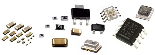
Figure 1 - SMD Componets In the early stages, SMD were soldered manually. Then the first batch of pick-and-place machines could only handle a few simple components. The more complex and smaller components still needed to be placed manually. Not long before the introduction of surface mount components over 20 years ago, a new era was born. From simple resistors to complex ICs, almost every through-hole component now has an SMT equivalent.
The actual process of SMT
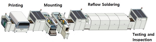
Figure 2 - SMT Components Sequence
In the 1980s, SMT production technology became increasingly more refined and as a result, is widely used in mass production. As costs were reduced and technical performance enhanced, more advanced but economical equipment became available. Types of SMD Passive components
Discrete components
Electromechanical devices
Where SMT and SMD combine In the early years of SMDs, smaller and more complex components had to be placed and hand soldered by an electronic manufacturer. Machines could do some of the pieces, limited to size and type. Today, manufacturing boards using SMT is somewhat similar, but much faster and far more accurate. Back then, small bits of silver or lead were placed on the board to attach the component. These elements are still used, but in a solder paste, which is a mixture of flux and small bits of solder. SMT machines can attach thousands of SMDs per hour, compared to maybe a few hundred by hand. Consequently, nearly every through-hole process now has an SMT equivalent. The popularity of SMDs came in response to how much more efficiently SMT could produce boards. The smaller component meant that both time and space could be maximized when both were used together. The SMD meant that more could be done with a smaller, more precise devise. And SMT could get them assembled more quickly and accurately than any process before. The cost savings combined has resulted in more and more electronics manufacturing services putting SMDs on an SMT. Reflow Soldering Reflow soldering is the process of melting and solidifying solder paste, which is currently in a semi-liquid condition. It helps create a strong solder connection. The SMT method often employs reflow soldering when working with small-pin parts like ball grid arrays. It allows for exact temperature control and consistent heat distribution, leading to excellent solder joints. For more dtails see Figure 3 and 4 below
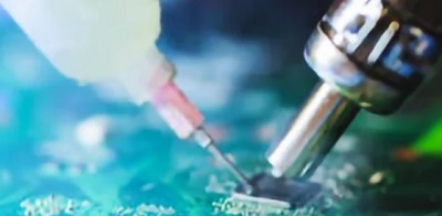
When working with these components it is always mandatory to use Soldering Flux . First of all the Soldering Flux helps to perform good welding, but is also very important to prevent damage to the slopes Normally should be use a medical syringe as shown in the Figure 5 below
Figure 5 - Syringe to inject the solder Flux
What Are the Major Elements of AOI? Fast and accurate quality control of PCBs is made possible with the help of image processing technology, which plays a significant role in inspection. In order to guarantee that their goods are of the best quality, companies operating in the 3C industry use advanced cameras, top-quality lenses, and image-processing software. The optical system serves a crucial role in an AOI system since it captures pictures of the target object. The system’s efficiency is proportional to the quality of these photos. The standard optical setup for an AOI includes a light source, lenses, and a camera. Light Source Product testing should take place in bright light conditions in the presence of a reliable light source. The success of flaw detection depends very much on the nature of the light source, the color of the light, and the orientation of the light source. Depending on the task, an AOI system can use a single light source or many sources. There was a time when companies used to employ various lighting options. Today’s setup mainly uses halogen lights and LED arrays to get light that is both steady and consistent.
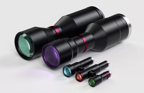
Lenses The system’s lenses focus the product’s reflected light onto the camera’s image sensor. To get clear photos, you need to have a collection of high-quality industrial lenses. The image resolution of the AOI device determines the precision of information it can detect and record. In other words, resolution is crucial since it determines how quickly and precisely an examination can be performed. Remember, the CCD imaging system is the foundation of the AOI system. The light source typically highlights the components under inspection. However, the important task, i.e., taking the picture, is performed by the lens, which then transmits it as a beam of light to the sensor. The quality of a pixel, or the quantity of information contained in a pixel, is mostly determined by the camera’s lighting system and lens. That’s why it is highly important to choose a better lighting system and advanced lenses. After lighting source, the success of your inspection operation depends on the type of lens you choose. For more details see Figure 6 below
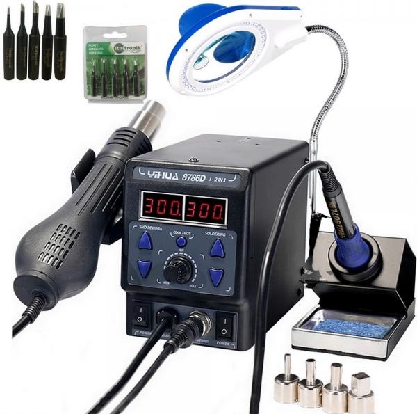
Figure 6 - Professional Lenses Normally in a professional desoldering station, all is included. For more details see Figure 7 below, is available here this fantastic and economical desoldering station
Figure 7 - Desoldering Station
Conclusion Working on this type of welding is not so easy, because the material to be removed or welded undergoes strong temperature stresses. For this reason, before using this station it is important to know the datasheet of the component that should be removed, and also the connection slopes on the PCB, and then act accordingly. |

+(39) 347 051 5328
Italy - Kazakhstan


09.00am to 18.00pm
About
We offer the best and economical solutions, backed by 27+ years of experience and international standards knowledge, echnological changes, and industrial systems.
Our Services
Marketing Materials


Marketing Materials1


