
Digital Logic Combinational Logic
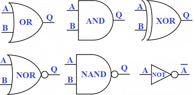
Combinational circuits are built of five basic logic gates:
There is a sixth element in digital logic, the inverter (sometimes called a NOT gate). Inverters aren’t truly gates, as they do not make any decisions. The output of an inverter is a 1 if the input is a 0, and vise versa.
A few things of note about the above image:
Digital logic circuits are usually represented using these six symbols; inputs are on the left and outputs are to the right. While inputs can be connected together, outputs should never be connected to one another, only to other inputs. One output may be connected to multiple inputs, however.
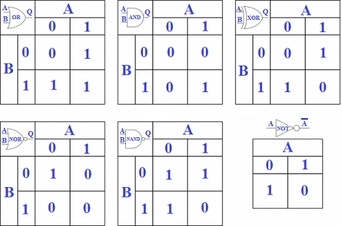
Truth Tables The descriptions above are adequate to describe the functionality of single blocks, but there is a more useful tool available: the truth table. Truth tables are simple plots which explain the output of a circuit in terms of the possible inputs to that circuit. Here are truth tables describing the six main elements:
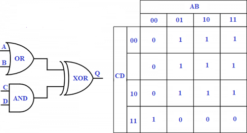
Truth tables can be expanded out to an arbitrary scale, with as many inputs and outputs as you can handle before your brain melts. Here’s what a four-input circuit and truth table look like:
Written Boolean Logic It is, of course, useful to be able to write in a simple mathematical format an equation representing a logical operation. To that end, there are mathematical symbols for the unique operations: AND, OR, XOR, and NOT.
You’ll note that there are two missing elements on that list: NAND and NOR. Typically, those are simply represented by complementing the appropriate representation:
Sequential Logic Combinational logic is great, but without adding sequential circuitry, modern computing would not be possible. Sequential circuitry is what adds memory to our logical systems. As mentioned earlier, combinational logic produces results after a delay. That delay varies according to lots and lots of things: the manufacturing process of the parts involved, the temperature of the silicon, the complexity of the circuit. If the output of a circuit is dependant upon results from two other combinational circuits and the results arrive at different times (which they will, in the real world), a combinational circuit will "glitch" briefly, outputting a result which may not be consistent with the desired operation. A sequential circuit, however, only samples and propagates the output at specific times. If the input changes between those times, it is ignored. The sampling time is usually synchronized across the entire circuit and is referred to as the "clock". When a computer's "speed" is cited, this is the value in question. It is possible to design "asynchronous" sequential circuits, which do not rely on a synchronized global clock. However, those systems pose great difficulties, and we won't be discussing them here. As a side note, any section of digital logic will have two characteristic delay values: the minimum delay time and the maximum delay time. If the circuit fails the minimum delay time (i.e., is faster than it should be), the circuit will fail, irreparably so. If that circuit is part of a larger device, like a computer CPU, the entire device is garbage and cannot be used. If the maximum delay time fails (i.e., the circuit is slower than it should be), the clock speed can be reduced to accommodate the slowest circuit in the system. Maximum delay times tend to go up as the silicon forming a circuit warms up, which is why computers become unstable when they overheat or as the clock speed is increased (as is the case with overclocking).
Sequential Circuit Elements As is the case with combinational logic, there are several basic circuit elements which form the building blocks of sequential circuits. These blocks are built up from the basic combinational elements, using feedback from the output to stabilize the input. They come in two "flavors": latches and flip-flops. While the terms are frequently used interchangeably, latches are generally less useful, as they are not clocked; we'll focus on flip-flops.
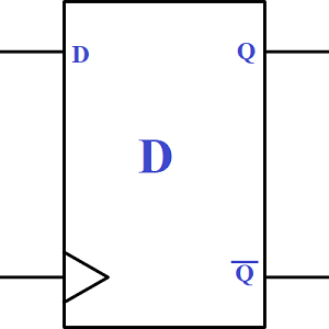
D-type Flip-Flop
The simplest type of flip-flop is the D-type. D flip-flops are simple -- upon a clock edge (normally rising, although they can be found with a built-in inverter to clock in on the falling edge instead), the input is latched to the output. Usually, the clock input is denoted by the small triangle impinging on the symbol. Most flip-flops provide two outputs: the "normal" output, and the complemented output.
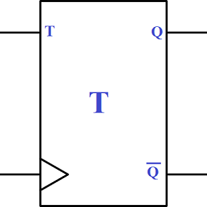
T-type Flip-Flop
Only slightly more complex is the T-type. The 'T' stands for "toggle." When a clock edge occurs, if the input T is a 1, the output changes state. If the input is a 0, the output remains the same. As with the D-type, the complement of the output is usually provided. A useful function of the T flip-flop is as a clock division circuit. If T is held high, the output will be the clock frequency divided by two. A chain of T flip-flops can thus be used to produce slower clocks from a device's master clock.
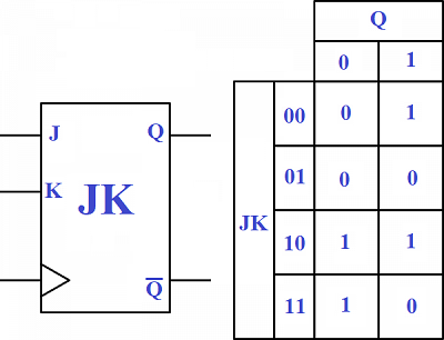
JK-type Flip-Flop
Finally, we have the JK-type. The JK-type is the only one of the three which truly requires a truth table to explain; it has two inputs (J and K), and the output can be left the same, set, cleared, or toggled, depending on the combination of input signals present. Of course, as with all flip-flops, the input at the moment of the clock is the only thing that matters
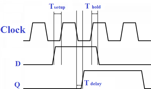
Setup, Hold, and Propagation Times All sequential circuits have what are called "setup" and "hold" times, as well as a propagation delay. Understanding these three things is critical to designing sequential circuits that work as expected. The setup time is the minimum amount of time before a rising clock edge occurs that a signal must arrive at the input of a flip-flop in order for the flip-flop to latch the data correctly. Likewise, the hold time is the minimum time a signal must remain stable after the rising clock edge occurs before it can be allowed to change. While setup and hold times are given as minimum values, the propagation delay is given as a maximum. Simply put, the propagation delay is the greatest amount of time after a falling edge at the clock before you can expect to see the signal on the outputs. Here's a graphic explaining them:
Note that in the above image, transitions are drawn as being slightly angled. This serves two purposes: it reminds us that clock and data edges are never truly right angles and will always have some non-zero rise or fall time, and it makes it easier to see where the vertical lines marking the various times intersect with the signals. The combination of these three values determines the highest clock speed a device may use. If the propagation delay of one part plus the setup time of the next part in the circuit exceeds the time between the falling edge of one clock pulse and the rising edge of the next, the data will not be stable on the input of the second component, causing it to behave in an unexpected manner.
Metastability Failing to adhere to setup and hold times can lead to a problem called "metastability". When a circuit is in a metastable state, the output of a flip-flop can oscillate rapidly between the two normal states -- often at a rate far above the clock rate of the circuit.
Metastability problems can range from spurious operation up to damage of the chip, since they can increase current consumption. While metastability usually resolves on its own, by the time it does so, the system may be in a totally unknown state and need to be completely reset to restore proper operation. A common way in which metastability issues arise is when a signal crosses clock domains -- in other words, when a signal passes between devices which are being clocked by different sources. Since the clocks are not synchronized (and even if the clocks are at the same nominal frequency, reality dictates that they will be slightly different), eventually a clock edge and a data edge are bound to be too close for comfort, resulting in a setup time violation. A simple fix for this issue is to run all inputs into a system through a pair of cascaded D flip-flops. Even if the first flip-flop goes into metastability, it will (hopefully) have settled down to a steady state before the next clock pulse, allowing the second flip-flop to read the correct data. This results in a one-cycle delay in incoming data edges, which is almost always insignificant compared to the risk of metastability.
below all others pages for digital logic:
|

+(39) 347 051 5328
Italy - Kazakhstan


09.00am to 18.00pm
About
We offer the best and economical solutions, backed by 27+ years of experience and international standards knowledge, echnological changes, and industrial systems.
Our Services
Marketing Materials


Marketing Materials1


