
|
Shift Registers what is the Shift Register ? Shift Registers are sequential logic circuits, capable of storage and transfer of data. They are made up of Flip Flops which are connected in such a way that the output of one flip flop could serve as the input of the other flip-flop, depending on the type of shift registers being created.
Shift registers are basically a type of register which have the ability to transfer (“shift”) data. Registers are generically storage devices which are created by connecting a specific number of flip flops together in series and the amount of data (number of bits) which can be stored by the register is always directly proportional to the number of flip flops, as each flip flop is capable of storing only one bit at a time. When the flip-flops in a register are connected in such a way that the output of one flip flop, becomes the input of the other, a shift register is created.
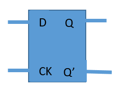
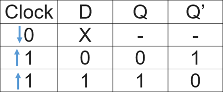
Flip Flops are devices with an operation similar to that of a latch. It can be referred to as a bistable vibrator which can move between two states (0 or 1) and is capable of storing data in bits. New data is read into a flip flop with each clock cycle and the previous data sent at the output. This however depends on the kind of flip flop, as the Input, Output, and clock cycle relationship between flip flops vary. There are different kinds of flip flops, but the most commonly used in the creation of shift registers are the D (Delay)-flip flops. For the operation of the D flip flops which makes them so desirable for shift registers, whenever there is a change on the clock of a D flip flop (either rising or falling edge, depending on the specifications of the flip flop). The data at the output “Q” becomes the same data as the one at the input “D”. The Output “Q” of the flip flop will stay at that value until the next clock cycle, where it will then change again to the value(High or low, 1 or 0) at the input.
Types of Shift Registers Shift registers are categorized into types majorly by their mode of operation, either serial or parallel. There are six (6) basic types of shift registers which are listed below although some of them can be further divided based on direction of data flow either shift right or shift left.
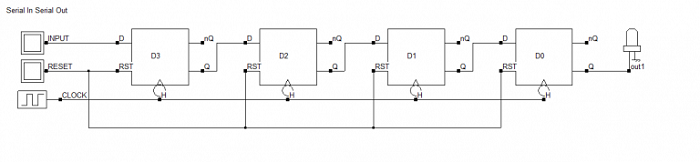
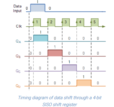
example: how can design a 4-bit Serial In Serial Out shift register (SISO) ? Okay, so we know that we have 4 D flip-flops. All of them have the same clock input. And all of them have the same reset input. Since we have a serial input, we will take only one input port. This input port is to the first flip-flop in the register. Similarly, since we are taking the output serially. We will have only one output which will be taken at the output pin of the last flip-flop. From the above configuration, our SISO shift register will look like this.
From the property of the D flip-flop, when we input a 1-bit signal “1”, it will be present at D1 flip-flops output at the rising edge of the first clock cycle. In the next clock cycle, it will be taken as input by the D2 flip-flop and will be available at Q2 output and so on. Furthermore, at the fourth clock pulse, we will get the 1-bit data “1” at the output Q4, having undergone a successful shift.
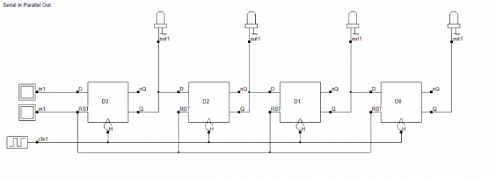
example: how can 4-bit Serial In Parallel Out shift register (SIPO)? Let’s take the four D flip-flops and take outputs from each individual flip-flop. That covers the parallel out part. Give a single input to the first flip-flop. Similarly, take a single output from the last flip-flop. Connect all the remaining flip-flops’ outputs to their subsequent flip-flops’ input. That settles the serial input part. Finally, apply the clock and the reset signal and voila you have your 4-bit SIPO shift register.
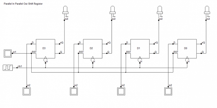
example: How to design a 4-bit Parallel in Parallel Out shift register (PIPO)? Again repeating the same approach we saw earlier, we will go ahead with cues from the title. Let’s straightaway connect the output ports (Q ports) of the D flip-flops to the output pins. The name suggests that we have parallel inputs too. Hence, we will connect the input ports (D ports) of the flip-flops to the input pins. Eventually, we will connect the clock ports to the clock input and the reset ports to the reset inputs. The resulting logic circuit for the 4-bit PIPO shift register is as follows.
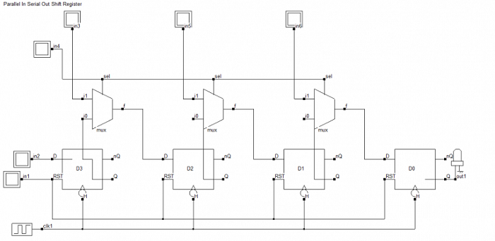
example: How to design a 4-bit Parallel in Serial Out shift register (PISO)? Things get a little bit tricky here. Mostly due to the fact that we need to share ports in order to achieve this configuration. The title requires us to have parallel inputs, which means that all the D ports will have their own independent input lines. And the title also requires us to have serial outputs. From the preceding designs, we have seen that a serial output means that data has to be taken out from only the final flip-flop. Moreover, the data needs to move through the series of flip-flops. This means that the outputs of flip-flops (Q ports) will also need to be connected to the inputs (D ports) of their subsequent flip-flops. This puts us in a pickle.
Dealing with multiple inputs The input ports need their separate input line as well as a connection from the previous flip-flops. How can we give two distinct signals to the same port? What can we use that would allow us to select from one of the two inputs that need to be given to the flip-flops? The answer is a multiplexer. A 2:1 multiplexer will allow us to choose between two inputs. So moving on to the construction of the PISO shift register. To begin with, let’s connect all the clock inputs and reset signals to their respective inputs. Then we know that we have a serial output so let’s connect the output of the last flip-flop to the output pin. The first flip-flop also does not need a serial input because there is no preceding flip-flop. So let’s give it its solitary input port. The remaining three flip-flops will have their inputs connected to the outputs of three multiplexers. Let’s go ahead and make that connection. Now, the multiplexers have two inputs. The first is the independent input that we require because we are making a parallel input shift register. Second, the output of the preceding flip-flop since we need a serial shift of data to get a serial output. The multiplexers also need a select input so that will be one extra input port. From the above configurations, we finally get a logic circuit for the 4-bit PISO shift register that looks like this:
Generally shift registers are available in 4000 series and 7000 series ICs.
4000 Series
7000 series
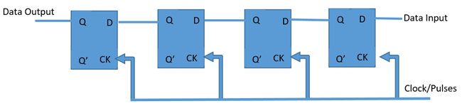
Serial in - Serial out Shift Registers Serial in – Serial out shift registers are shift registers that streams in data serially (one bit per clock cycle) and streams out data too in the same way, one after the other.
A simple serial in – serial Out 4-bit shift register is shown above, the register consists of 4 flip flops and the breakdown of how it works is explained below; On startup, the shift register is first cleared, forcing the outputs of all flip flops to zero, the input data is then applied to the input serially, one bit at a time. There are two basic ways of shifting data out through a shift register;
Non-Destructive Readout Non - Destructive readout based, shift registers always have a read/write mode of operation with an extra line added to allow the switch between the read and write operational modes. When the device is in the “write” operational mode, the shift register shifts each data out one bit at a time behaving exactly like the destructive readout version and data is thus lost, but when the operational mode is switched to “read”, data which are shifted out at the input goes back into the system and serve as input to the shift register. This helps ensure that the data stays longer (as long as it stays in read mode)
Destructive Readout For destructive readouts, the data is completely lost as the flip flop just shifts the information through. Assuming for the 4-bit shift register above, we want to send the word “1101”. After clearing the shift register, the output of all the flip flops becomes 0, so during the first clock cycle as we apply this data (1101) serially, the outputs of the flip flops look like the table below.
First clock cycle:
Second clock cycle:
Third Clock Cycle:
Fourth Clock Cycle:
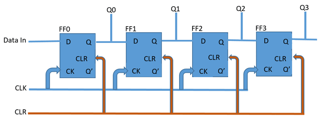
Serial in – Parallel out Shift Register The second type of shift register we will be considering is the Serial in – Parallel out shift register. These types of shift registers are used for the conversion of data from serial to parallel. The data comes in one after the other per clock cycle and can either be shifted and replaced or be read off at each output. This means when the data is read in, each read in bit becomes available simultaneously on their respective output line (Q0 – Q3 for the 4-bit shift register shown below). A 4-bits serial in – Parallel out shift register is illustrated in the Image below.
A table showing how data gets shifted out of serial in –parallel out 4 bit shift register is shown below, with the data in as 1001.
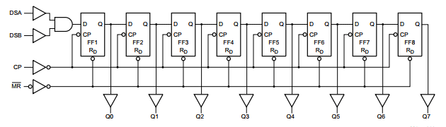
A good example of the serial in – parallel out shift register is the 74HC164 shift register, which is an 8-bit shift register. The device features two serial data inputs (DSA and DSB), eight parallel data outputs (Q0 to Q7). Data is entered serially through DSA or DSB and either input can be used as an active HIGH enable for data entry through the other input. Data is shifted on the LOW-to-HIGH transitions of the clock (CP) input. A LOW on the master reset input (MR) clears the register and forces all outputs LOW, independently of other inputs. Inputs include clamp diodes. This enables the use of current limiting resistors to interface inputs to voltages in excess of VCC.
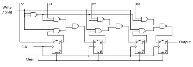
Parallel in – Serial out Shift Register For this type of shift register, the data is supplied in parallel, for example consider the 4-bit shift register shown below.
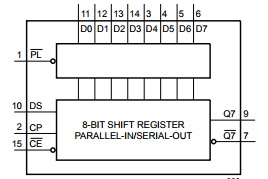
This register can be used to store and shift a 4-bit word, with the write/shift (WS) control input controlling the mode of operation of the shift register. When the WS control line is low (Write Mode), data can be written and clocked in via D0 to D3. To shift the data out serially, the WS control line is brought HIGH (Shift mode), the register then shifts the data out on clock input. A good example of a parallel in – serial out shift register is the 74HC165 8-bit shift register although it can also be operated as a serial in – serial out shift register. The device features a serial data input (DS), eight parallel data inputs (D0 to D7) and two complementary serial outputs (Q7 and Q7’). When the parallel load input (PL) is LOW the data from D0 to D7 is loaded into the shift register asynchronously. When PL is HIGH data enters the register serially at DS. When the clock enable input (CE) is LOW data is shifted on the LOW-to-HIGH transitions of the CP input. A HIGH on CE will disable the CP input. Inputs are overvoltage tolerant to 15 V. This enables the device to be used in HIGH-to-LOW level shifting applications. The functional diagram of the shift register is shown below;
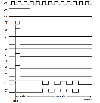
The timing diagram for the system is as shown in the image below;
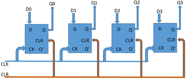
Parallel in – Parallel out shift register For parallel in – parallel out shift register, the output data across the parallel outputs appear simultaneously as the input data is fed in.
The input data at each of the input pins from D0 to D3 are read in at the same time when the device is clocked and at the same time, the data read in from each of the inputs is passed out at the corresponding output (from Q0 to Q3). The 74HC195 shift register is a multipurpose shift register which is capable of working in most of the modes described by all the types we have discussed so far especially as a parallel in – parallel out shift register.
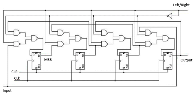
Bidirectional Shift Registers Shift registers could either perform right or left data shift, or both depending on the kind of shift register and their configuration. In right shift operations, the binary data is divided by two. If this operation is reversed, the binary data gets multiplied by two. With suitable application of combinational logic, a serial shift register can be configured to perform both operation. Consider the 4-bits register in the image below. A couple of NAND gates are configured as OR gates and are used to control the direction of shift, either right or left.
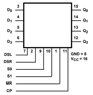
The control line left/write is used to determine the direction to which data is shifted, either right or left. The 74HC194 Bi-direction shift register is a good example. The register can operate in all the modes and variations of serial and parallel input or output. The functional diagram of the 74HC194 highlighting the control line, clock, input and output pins is shown below.
74Hc194 Shift register Functional Diagram
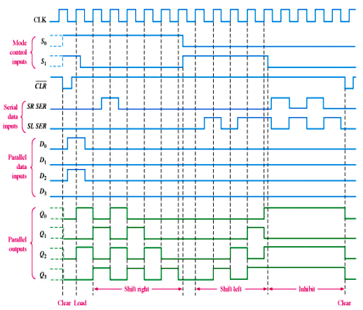
The timing diagram of the device is also shown below. It will better help you understand how the control line controls the actions of the register.
74HC194 Bidirectional Shift Register Timing Diagram
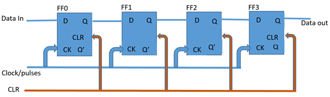
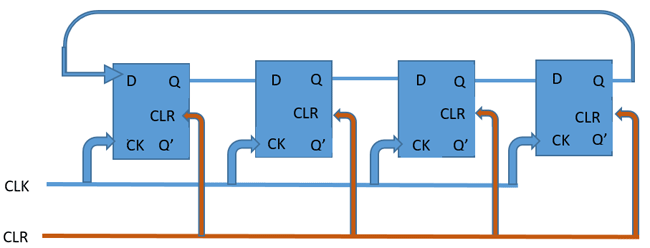
Counters Counters, sometimes called rotate shift register are basically shift registers with their outputs fed back into the device as inputs in such a way that it creates a particular pattern. These kinds of registers are referred to as counters because of the pattern and sequence they exhibit. This most popular type of shift register counters are the ring counters. Ring Counter Ring counters are basically a type of counter in which the output of the most significant bit is fed back as an input to the least significant bit. A 4-bit ring counter is illustrated in the diagram below using D flip flops.
4-bit Ring counter When the clock pulse is applied, the output of each stage is shifted to the next one, and the cycle keeps going. When clear is turned high, all the flip flops except the first one (which gets set to 1) is reset to zero.
Applications of Shift registers Shift registers are used in a lot of applications some of which are;
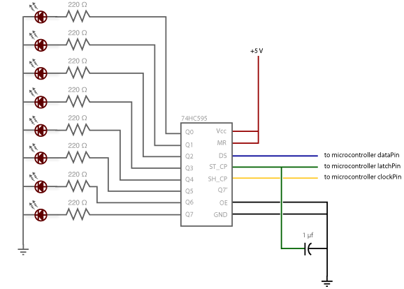
Reducing the required MCU's IO pins using a shift register
The time delay is usually calculated using the formula; t = N * (1 / fc) N is the number of flip flop stage at which the output is taken, Fc is the frequency of the clock signal and t which is the value being determined is the amount of time for which the output will be delayed. When selecting a shift register for a particular task because of the wide range and type its important to select one that matches your particular need, considering things like, the mode of operation, the bit size (number of flip flops), right or left or bidirectional etc.
www.bennypass.it |

+(39) 347 051 5328
Italy - Kazakhstan


09.00am to 18.00pm
About
We offer the best and economical solutions, backed by 27+ years of experience and international standards knowledge, echnological changes, and industrial systems.
Our Services
Marketing Materials


Marketing Materials1


