
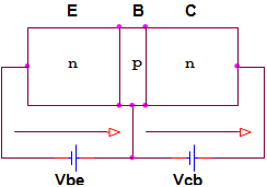
Characteristic of BJT transistors Introduction A Bipolar Junction Transistor (also known as a BJT or BJT Transistor) is a three-terminal semiconductor device consisting of two p-n junctions which are able to amplify or magnify a signal. It is a current controlled device. The three terminals of the BJT are the base, the collector and the emitter. A BJT is a type of transistor that uses both electrons and holes as charge carriers. A signal of small amplitude if applied to the base is available in the amplified form at the collector of the transistor. This is the amplification provided by the BJT. Note that it does require an external source of DC power supply to carry out the amplification process. Below the photo with all details
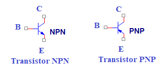
Working Principle There are two types of bipolar junction transistors – NPN transistors and PNP transistors. A diagram of these two types of bipolar junction transistors is given below.
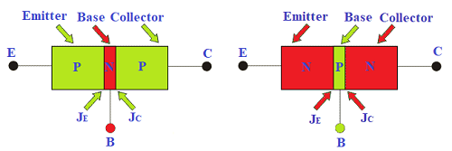
From the above figure, we can see that every BJT has three parts named emitter, base and collector. JE and JC represent the junction of emitter and junction of collector respectively. Now initially it is sufficient for us to know that emitter based junction is forward biased and collector-base junctions are reverse biased. The next topic will describe the two types of these transistors.
NPN Bipolar Junction Transistor In an n-p-n bipolar transistor (or npn transistor) one p-type semiconductor resides between two n-type semiconductors the diagram below an n-p-n transistor is shown
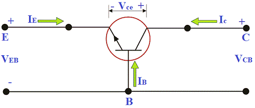
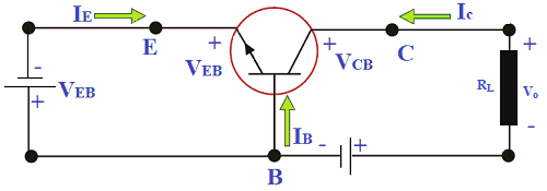
Now IE, IC is emitter current and collect current respectively and VEB and VCB are emitter-base voltage and collector-base voltage respectively. According to the convention if for the emitter, base and collector current IE, IB and IC current goes into the transistor the sign of the current is taken as positive and if current goes out from the transistor then the sign is taken as negative. We can tabulate the different currents and voltages inside the n-p-n transistor.
PNP Bipolar Junction Transistor Similarly for p-n-p bipolar junction transistor (or pnp transistor), an n-type semiconductor is sandwiched between two p-type semiconductors. The diagram of a p-n-p transistor is shown below
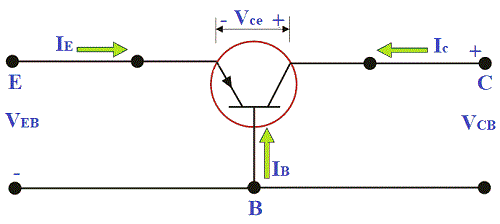
For p-n-p transistors, current enters into the transistor through the emitter terminal. Like any bipolar junction transistor, the emitter-base junction is forward biased and the collector-base junction is reverse biased. We can tabulate the emitter, base and collector current, as well as the emitter-base, collector base and collector-emitter voltage for p-n-p transistors also.
Working Principle of BJT Transistor The BE junction is forward bias and the CB is a reverse bias junction. The width of the depletion region of the CB junction is higher than the BE junction. The forward bias at the BE junction decreases the barrier potential and produces electrons to flow from the emitter to the base and the base is a thin and lightly doped it has very few holes and less amount of electrons from the emitter about 2% it recombine in the base region with holes and from the base terminal it will flow out. This initiates the base current flow due to the combination of electrons and holes. The leftover large number of electrons will pass the reverse bias collector junction to initiate the collector current. By using KCL we can observe the mathematical equation IE = IB + IC The base current is very less as compared to emitter and collector current IE ~ IC Here the operation of PNP transistor is the same as the NPN transistor the only difference is only holes instead of electrons. The below diagram shows the PNP transistor of the active mode region.
Advantages of BJT Transistor
Applications of BJT Following are the two different types of applications in BJT they are
Conclusion The semiconductor crystals that make up the emitter and the collector are doped with pentavalent material (type n) and the base with trivalent material (type p). The base is very thin (in the order of the micron). An important difference between the collector and the emitter is represented by the different doping values. The heavily doped emitter performs the function that, if the base-emitting junction is directly polarized, injects electrons into the base. Some electrons injected by the emitter into the base are recomposed with the few gaps present, being the base equipped with a few p-type atoms dopants and forming the base-emitter current. This mechanism can also be seen other way: If a current Ib it will go in the base-emitter junction, then the emitter emits electrons which, due to the minimum thickness of the base, can reach the collector and form a current Ic much larger than Ib. A transistor of this is called bipolar (BJT) because the conduction takes place both for the majority carriers in the emitter and collector and for minority bearers in the base. As you know there are two types of transistors: the NPN and PNP, both are show in the Figures above. They differ from each other by the design of the emitter, whose arrow for the PNP type indicates that inject holes into the base, and viceversa the NPN (see Figure below)
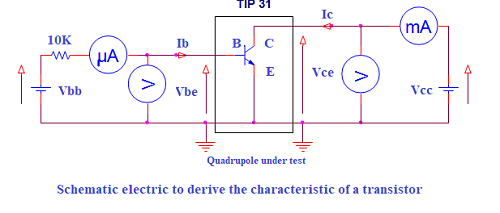
Considering the transistor as a black box it can be defined as a quadripolo having two input terminals and two output terminals. For its use it is therefore necessary to know the characteristics of entry and exit.
The behavior of the transistor connected in this way is as follows: by passing a small current Ib into the base, a large current flow Ic is obtained on the collector. The amplification ratio is defined as: bf = hFE = Ic/Ib
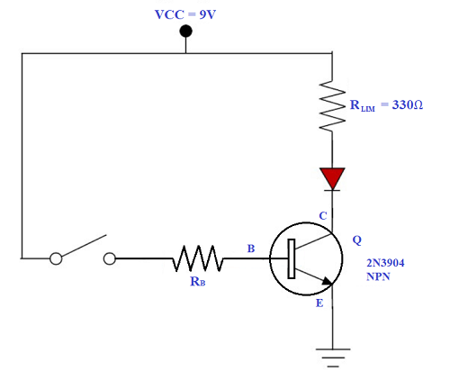
Common Practical Examples of Transistor as a Switch Transistor to Switch the LED The schematic below shows how a transistor is used to switch the Light Emitting Diode (LED).
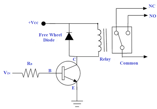
Transistor to Operate the Relay It is also possible to control the relay operation using a transistor. With a small circuit arrangement of a transistor able to energise the coil of the relay so that the external load connected to it is controlled.
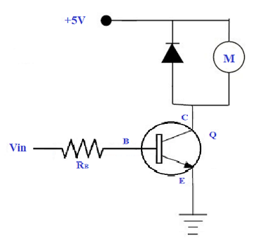
Transistor to Drive the Motor
Below automatic calculation power Transistors
www.bennypass.it |

+(39) 347 051 5328
Italy - Kazakhstan


09.00am to 18.00pm
About
We offer the best and economical solutions, backed by 27+ years of experience and international standards knowledge, echnological changes, and industrial systems.
Our Services
Marketing Materials


Marketing Materials1


