
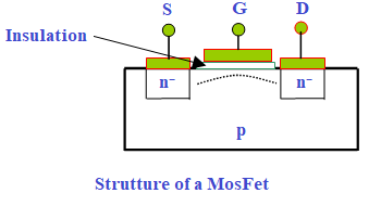
MOSFET and BJT Transistor (The Difference) The Mosfet transistor is another type of semiconductor "device" which is nowadays widely used above all in the logic circuits of computers, memories, CPUs, etc.Unlike the BJT transistor, which requires a base current as a command, the Mosfet is driven by a voltage.The structure of an enriched n-channel MosFet transistor is shown in the Figure below
Characteristics between Transistors BJT and MosFet The Transistors BJT & MOSFET are electronic semiconductor devices that give a large changing electrical o/p signal for small variations in small i/p signals. Due to this feature, these transistors are used as either a switch or an amplifier. The first transistor was released in the year 1950 and it can be treated as one of the most essential inventions of the 20th century. It is quickly developing the device and also various kinds of transistors have been introduced. The first type of transistor is BJT (Bipolar Junction Transistor) and MOSFET (Metal Oxide Semiconductor Field Effect Transistor) is another type of transistor introduced later. For a better understanding of this concept, here this article gives the main difference between BJT andMOSFET.
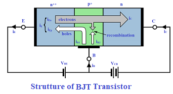
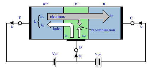
BTJ Transistor A bipolar junction transistor is one type of semiconductor device and in the olden days, these devices are used in the place of vacuum tubes. The BJT is a current-controlled device where the o/p of the base terminal or emitter terminal is a function of the current in the base terminal. Fundamentally, the operation of a BJT transistor is determined by the current at the base terminal. This transistor consists of three terminals namely the emitter, base, and collector. Actually, a BJT is a silicon piece that includes three regions and two junctions. The two regions are named the P-junction and N-junction. There are two kinds of transistors namely PNP and NPN. The main difference between BJT and MOSFET is their charge carriers. In the PNP transistor, P stands for positive and the majority charge carriers are holes whereas in the NPN transistor, N stands for negative and the majority charge carriers are electrons. The operating principles of these transistors are practically equal and the main difference is in biasing as well as the polarity of the power supply for each type. BJTs are apt for low current applications like switching purposes
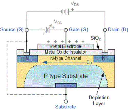
The Mosfet The MOSFET is one kind of FET (Field Effect Transistor), which consists of three terminals namely gate, source, and drain. Here, the drain current is controlled by the voltage of the gate terminal Therefore, these transistors are voltage-controlled devices. These transistors are available in 4 different types such as P-channel or N-channel with either an enhancement mode or depletion mode. The source and Drain terminals are made of N-type semiconductor for N-channel MOSFETs and equally for P-channel devices. The gate terminal is made of metal and detached from source & drain terminals using a metal oxide. This insulation roots low power consumption & it is a benefit in this transistor. Therefore, this transistor is used where p and n channel MOSFETs are used as building blocks to reduce the power consumption like digital CMOS logic. MOSFETs are classified into two types such as enhancement mode and depletion mode
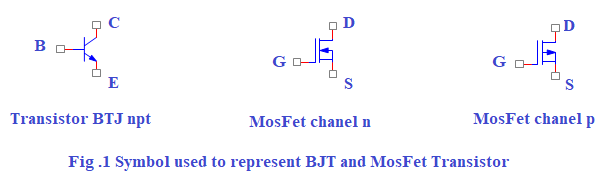
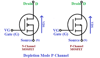
Below the figure 1 show the symbols of BJT and mosfet
Working Principle of BJT The working principle of a BJT involved the use of Voltage between the two terminals such as base and emitter to regulate the flow of current through the collector terminal. For instance, the configuration of a common emitter is shown in the figure below.
The change in voltage affects the current entering in a Base terminal and this current will, in turn, affect the o/p current called. By this, it is shown that the input current controls the flow of o/p current. So this transistor is a current controlled device. Please follow the below link to know more about; the Major Difference between BJT and FET.
Working Principle of MosFet The working of MOSFET depends upon the MOS (metal oxide capacitor) which is the essential part of the MOSFET. The oxide layer presents, among the two terminals such as source and drain. By applying +Ve or –Ve gate voltages, we can set from p-type to n-type. When +Ve voltage is applied to the gate terminal, then the holes existing under the oxide layer with a repulsive force and holes are pushed down through the substrate. The deflection region occupied by the bound –Ve charges which are associated with the acceptor atoms.
One of the most important things is to understand the difference between the BTJ and the MosFet, below all details
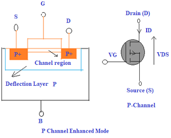
P-Channel MOSFET The P- channel MOSFET has a P- Channel region located in between the source and drain terminals. It is a four-terminal device having the terminals as gate, drain, source, and body. The drain and source are heavily doped p+ region and the body or substrate is of n-type. The flow of current is in the direction of positively charged holes. When we apply the negative voltage with repulsive force at the gate terminal, then the electrons present under the oxide layer are pushed downwards into the substrate. The depletion region populated by the bound positive charges which are associated with the donor atoms. The negative gate voltage also attracts holes from the p+ source and drain region into the channel region. Below the Figure with all details
N-Channel MOSFET The N-Channel MOSFET has an N- channel region located in between the source and drain terminals. It is a four-terminal device having the terminals as gate, drain, source, body. In this type of Field Effect Transistor, the drain and source are heavily doped n+ region and the substrate or body are of P-type. The current flow in this type of MOSFET happens because of negatively charged electrons. When we apply the positive voltage with repulsive force at the gate terminal then the holes present under the oxide layer are pushed downward into the substrate. The depletion region is populated by the bound negative charges which are associated with the acceptor atoms. Upon the reach of electrons, the channel is formed. The positive voltage also attracts electrons from the n+ source and drain regions into the channel. Now, if a voltage is applied between the drain and source the current flows freely between the source and drain and the gate voltage controls the electrons in the channel. Instead of positive voltage if we apply negative voltage then a hole channel will be formed under the oxide layer. 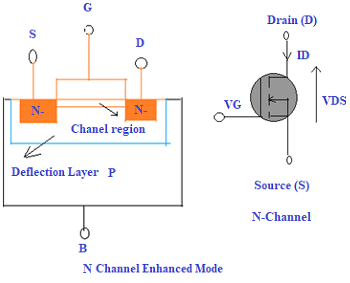
Temperature Coefficient of BJT & FET The temperature coefficient of MOSFET is positive for resistance and this will make MOSFET’s parallel operation very simple easy. Primarily, if a MOSFET transmits amplified current, very easily it heats up, increases its resistance, and causes this flow of current to move to other devices within parallel. The temperature coefficient of BJT is negative, so resistors are essential throughout the parallel process of the bipolar junction transistor. The secondary breakdown of MOSFET does not happen since the temperature coefficient of this is positive. However, bipolar junction transistors have a negative temperature coefficient so it results in a secondary breakdown.
MOSFET Regions of Operation To the most general scenario, the operation of this device happens mainly in three regions and those are as follows:
Let us now consider the switching characteristics of MOSFET A semiconductor too such as MOSFET or Bipolar Junction Transistor is basically functioned as switches in two scenarios one is ON state and the other is OFF state. To consider this functionality, let us have a look at the ideal and practical characteristics of the MOSFET device. Ideal Switch Characteristics When a MOSFET is supposed to function as an ideal switch, it should hold the below properties and those are
Practical Switch Characteristics As the world is not just stuck to ideal applications, the functioning of MOSFET is even applicable for practical purposes. In the practical scenario, the device should hold the below properties
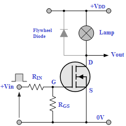
Example of MOSFET as a Switch In the below circuit arrangement, an enhanced mode and N-channel MOSFET are being used to switch a sample lamp with the conditions ON and OFF. The positive voltage at the gate terminal is applied to the base of the transistor and the lamp moves into ON condition and here VGS =+v or at zero voltage level, the device turns to OFF condition where VGS=0.
If the resistive load of the lamp was to be replaced by an inductive load and connected to the relay or diode which is protected to the load. In the above circuit, it is a very simple circuit for switching a resistive load such as a lamp or LED. But when using MOSFET as a switch either with inductive load or capacitive load, then protection is required for the MOSFET device. If in the case when the MOSFET is not protected, it may lead to damage of the device. For the MOSFET to operate as an analog switching device, it needs to be switched between its cutoff region where VGS =0 and saturation region where VGS =+v. MOSFET can also function as a transistor and it is abbreviated as Metal Oxide Silicon Field Effect Transistor. Here, the name itself indicated that the device can be operated as a transistor. It will have P-channel and N-channel. The device is connected in such a way using the four source, gate, and drain terminals and a resistive load of 24Ω is connected in series with an ammeter, and a voltage meter is connected across the MOSFET. In the transistor, the current flow in the gate is in a positive direction and the source terminal is connected to ground. Whereas in bipolar junction transistor devices, the current flow is across the base-to-emitter path. But in this device, there is no current flow because there is a capacitor at the beginning of the gate, it just requires only voltage. This can be happened by proceeding with the simulation process and by switching ON/OFF. When the switch is ON there is no current flow across the circuit, when the resistance of 24Ω and 0.29 of ammeter voltage are connected, then we find the negligible voltage drop across the source because there is +0.21V across this device. The resistance between drain and source is termed as RDS. Due to this RDS, the voltage drop appears when there is current flow in the circuit. RDS varies based on the type of the device (it can vary in between 0.001, 0.005, and 0.05 based on the type of voltage.
Advantages of BJT over MOSFET The advantages of BJT over MOSFET include the following.
The disadvantages of BJT include the following.
Advantages and Disadvantages of MOSFET
The disadvantages of MOSFET include the following.
Conclusion
There are few conditions to be observed while selecting the MOSFET as a switch and those are a follows:
The main restriction at the time of operating MOSFET as a switching device is the enhanced drain current value that the device can be capable of. It means that RDS in ON condition is the crucial parameter which decides the switching capability of the MOSFET. It is represented as the ratio of drain-source voltage to that of drain current. It has to be calculated only in the ON state of the transistor.
In general, a boost converter needs a switching transistor for the operation of the device. So, as switching transistor MOSFETs are used. These devices are used to know the current value and voltage values. Also, considering the switching speed and cost, these are extensively employed. In the same way, MOSFET can also be used in multiple ways. and those are
The MOSFET is very important part of electronics. Pratically is used for multiple application like as:
www.bennypass.it
|

+(39) 347 051 5328
Italy - Kazakhstan


09.00am to 18.00pm
About
We offer the best and economical solutions, backed by 27+ years of experience and international standards knowledge, echnological changes, and industrial systems.
Our Services
Marketing Materials


Marketing Materials1


