
|
OPERATIONAL AMPLIFIERS
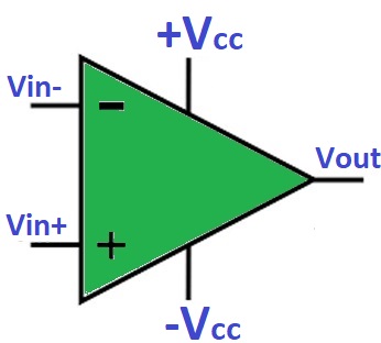
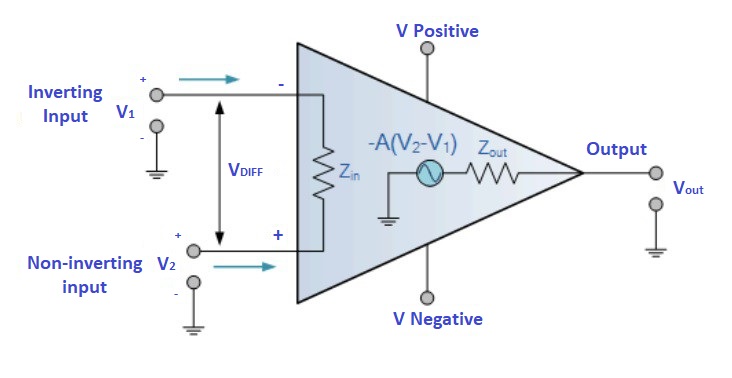
Introduction The operational amplifiers are circuit elements used in many applications, from signal amplifiers to signal conditioning and filtering, from circuits that perform mathematical operations on the comparator signal. Possible to be realized also with discrete transistors, they are found in various packages as integrated circuits. The operational amplifier is a fundamental element, able to amplify a voltage, with 3 essential pins, the non-inverting pin, in pin inverting is the output. To these three pins we need to add the two pins for the power supply. The inverting and non-inverting pins are high-impedance inputs, that is they do not absorb current. They are indicated with the symbol "+" and the symbol "-" respectively. The output is low impedance and is able to supply and absorb curren The output signal is given by the difference between input V1 and input V2 multiplied by an amplification factor A which is usually very large and depends on the operational amplifier and not on the circuit created therewith. Usually this value goes from 20K to 200K and theoretically is infinite and is called an open loop gain. If A = infinity then the difference between the inverting and the non-inverting pins must be infinitesimal, theoretically 0, otherwise the output voltage would immediately saturate, functioning as a comparator. For this reason that A >> 1, then, we have the principle of virtual short-circuit, which causes the same voltage on the inverting and non-inverting pins. The operational amplifier can perform its amplification functions, mathematical operations and filtering using a negative feedback, that is part of the output voltage returns to the inputs limiting the gain and allowing use without the outputs saturating. Theoretically, an operational amplifier is as follows:
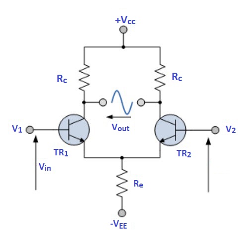
The two transistors are connected in differential configuration and are of the same type and operate in the same working point. The output voltage Vout is given by (V2-V1) A then the function seen above is performed. This happens because when V1 is greater than V2 the transistor T1 is more on and therefore the Vout will see a lower voltage on TR1 and a higher voltage on TR2 creating a negative Vout. When choosing an operational amplifier there are several factors to consider, all detail below:
When analyzing a circuit with an operational amplifier, the ideal model of the component is considered, therefore with null input currents, virtual short circuit and output schematized as a generator without series resistance. The input current is nothing in reality, so we will see how to reduce this influence. Furthermore until now we have not considered the supply voltage; Obviously the output signal can never be higher than the supply voltage, that is if I have 1V input and 10 times the output amplify I will have 10V only if the power is higher than 10V or the same maximum in the case of operational amplifiers " rail to rail ". Therefore, the maximum output signal in the module (both positive and negative) cannot be greater than the supply voltage.
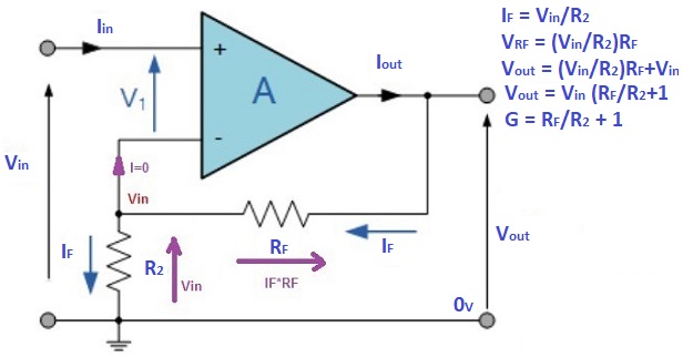
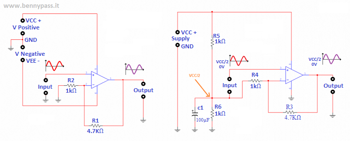
NON-INVERTING AMPLIFIER For non-inverting amplifier we mean an amplifier that performs a positive-value amplification function, i.e. we will have Vout = G * Vin. To perform this function you need an operational and two resistors:
In doing so, we find it in the non-inverting pin. A current is then created in R2 given by Vin / R2. Since in the non-inverting pin no current flows (I = 0) Vin / R2 coincides with IF, IF flows in RF and creates a voltage drop given by (Vin / R2) IF. These two voltage add up then Vout = Vin + (Vin / R2) RF = Vin (1 + RF / R2). The gain is defined as Vout / Vin, so the gain in this case is G = (1 + RF / R2). As for the power supply the scheme works both with dual and single power supply except for some integrated. With a small modification it works with single power supply every operational amplifier. The various circuits for each application ar
In the image above you can see first a non-inverting amplifier with dual power supply and equal gain G = (1 + 4.7 / 1) = 5.7. As for the power supply it is dual or composed of a central ground terminal and two other wires one with positive voltage and one with negative voltage with respect to the mass. For example, you can have + 12V and -12V. In the second image there is only one power supply, then single, with positive and GND. To create a fictitious mass, two resistors and a C1 capacitor are used. At the terminals of C1 due to the resistive divider between R5 and R6 there will be a voltage equal to VCC / 2 or half power supply. Thus the input waveforms oscillate around VCC / 2. Measuring the output with zero input voltage will not have 0 V but VCC / 2. The gain and the waveform of the output are the same as the previous case. The above schemes are ideal for sinusoidal input voltages, ie with a positive and negative signal. If sensors like LM35 are used, it returns a positive only voltage that can be amplified as follows:
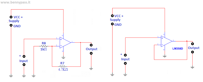
In the first scheme there is always a gain of 4.7 times so if the sensor generates 100mV output I will find 470mV. This scheme is used to couple sensors to ADC converters, for example. The second image is a BUFFER or a non-inverting amplifier with unit gain. It has therefore gain 1 and even if it seems useless it is very useful if for example the input signal comes from a sensor with high output resistance. To avoid degrading the signal, the circuit seen in the second image is used. The second scheme also works with dual power supply as well as operating with single power supply.
INVERTING AMPLIFIER For inverting amplifier we mean an amplifier that performs a negative value amplification function, that is we will have Vout = -G * Vin. The minus sign means only a phase inversion; if I amplify a sinusoidal signal I will always output a sinusoidal signal but inverted by 180 ° or if the first half-wave input is positive at the output we will have a negative half-wave, if instead I amplify a DC voltage of 3V for example in the output had a negative voltage , for example -15V if the amplifier has a gain equal to 5. To perform this function serve as in the previous case an operational and two resistors:
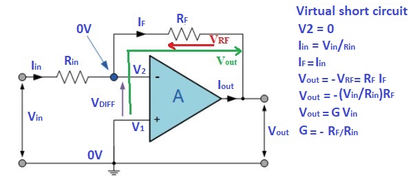
Consider the theoretical principles seen above; we will have that for the virtual short circuit V2 is 0, that is, on the two inputs there will be the same voltage and also in the inverting and non-inverting pin it does not flow current. In doing so Rin will have Vin and the masses to the leaders, then flows in it a current given by Iin = Vin / Rin. Since the current "Iin" does not flow in the inverting terminal of the operational amplifier, it has no other branch in which to flow except in the "RF" branch. In "RF", due to the current, a voltage drop is created due to VRF = RF IF = RF Iin. The "Vout" due to the virtual short circuit is also equal to VRF, however, since Vout has the tip on the output node while the VRF has the tip to the contrary then the Vout = -VRF. Combining the equations of "Iin" with that of the "Vout" voltage we obtain that Vout = -Vin (RF / Rin) and consequently the gain will be equal to G = - (RF / Rin). As for the power supply the scheme works both with dual and single power supply except for some integrated. With a small modification it works with single power supply every operational amplifier. The various circuits for each application are:
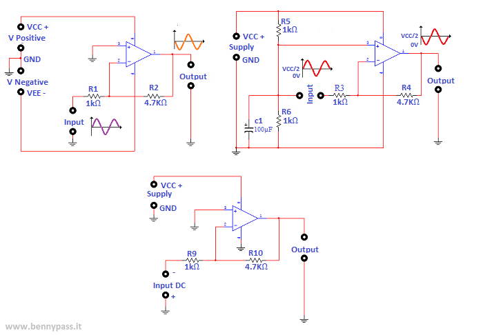
The first scheme represents an inverting amplifier with dual supply voltage. The input can be either an alternating or direct voltage source. The gain will be G = -R2 / R1 = 4.7 times. Given the negative gain, the incoming waveform is reversed as shown. In the second image the power supply is single but a virtual mass is created at VCC / 2 value in order to simulate a dual power supply. The input signal and the output voltage do not oscillate around 0V but oscillate around the VCC / 2 value. The third scheme represents an amplifier with single power supply and input in direct voltage. Obviously, since the power supply is only positive, negative values cannot be output and, given the negative sign of the gain, the input voltage must be negative. The first scheme works with any input.
www.bennypass.it |

+(39) 347 051 5328
Italy - Kazakhstan


09.00am to 18.00pm
About
We offer the best and economical solutions, backed by 27+ years of experience and international standards knowledge, echnological changes, and industrial systems.
Our Services
Marketing Materials


Marketing Materials1


