
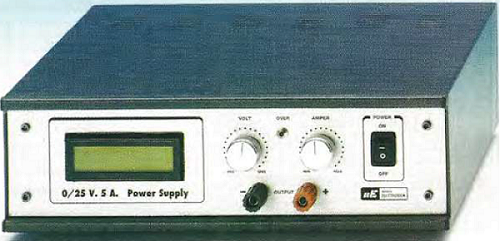
Professional power supply
The instrument that we propose is very reliable; for this reason, the name is professional laboratory power supply. The output voltage is precise and stable, freely adjustable from 0 to 25 volts according to the particular needs; it also includes current limitation adjustable according to the needs up to 5 amps maximum. This function is to avoid problems in the event of a short circuit.
Wiring Diagram
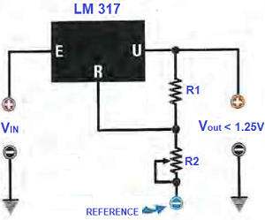
Figure 2 Wiring Diagram Observing the wiring diagram drawing shown in fig. 2 makes it easy to recognize the three secondaries of transformer T1. The first from the top provides the 14 +14 volts alternating, which provides an alternating voltage of 28 volts, that will be used for output voltages greater than 12 volts. The alternating voltage of 14 volts, it's used instead for output voltages less than 12 volts. These two different voltages are automatically selected by the contacts of Relay 1, which we have reported only the internal contact on the secondary. This relay is fully visible at the bottom left in the diagram of fig.2. We also find a secondary with 28 volts alternating which is used to power the MFT1 MOSFET. This MOSFET acts as a switch and acting exclusively in the power supply shutdown phase and preventing a dangerous voltage spike on the output terminals due to the negative reference voltage goes to zero before the voltage stored in the capacitors C7 Finally, from the last secondary, which is 10 volts of alternate, we can obtain from diode DS4, the electrolytic C11, the stabilizer IC1, the 5 continuous volts to power the display board, to see the voltage and the ampere from it. From the same secondary, we also obtain through the diode DS3, the electrolytic C12, and the stabilizer IC2, a negative voltage that becomes the negative voltage reference from -2 volts to -6 volts continuous which sent to the R pin of lC3 (LM317) to regulate the general output voltage. If we did not drive the IC3 voltage regulator with a negative voltage, due to a reference inside it, would provide a minimum output voltage of 1.25 volts and not 0 volts, as we set out to design this power supply. Once the instrument is mounted, the test point TP1, which is connected on pin 3 of IC2, allows us to verify that the stage composed of IC2 will work. In the wiring diagram of fig. 2, we have marked a negative voltage of 6 volts corresponding with TP1, a purely indicative value because you could also detect slightly higher or lower values. To lower the minimum voltage which can be taken from the U pin of the LM317 to 0 volts, we applied the design principle exemplified in the diagrams as shown in Fig. 3-4.
In the first diagram (see fig. 3), the integrated LM317 stabilizer can regulate the voltage from the maximum input voltage minus 3 - 4 volts up to a minimum of 1.25 volts through the divider formed by R1 and R2. Usually, for R2 which is a potentiometer, an ohmic value of 4,700 ohms is used, while the resistance R1 is 220 ohm
Voltage Control The regulation of the output voltage is entrusted to the IC3 stabilizer. If the output voltage is set to be greater than 12 volts, the voltage comparator IC5 excites RELE 1 by connecting the alternating voltage of 28 volts to the RS1 rectifier bridge. If the output voltage is less than 12 volts, the voltage comparator IC5 de-energizes RELE 1 by connecting the 14volt voltage to the rectifier bridge RS1. This automatic system avoids that for strong low voltage absorption, the transistors have to dissipate the excess voltage in the heat in case of strong low voltage absorption. In fact, if with a continuous 24volt power supply, we will power a device that absorbs 1 ampere at 12 volts, we must dissipate well: (24 - 12) x 1 = 12 watts in heat If, on the other hand, to power the same device, we use a 13volt continuous power supply, we only have to dissipate: (13 - 12) x1 = 1 watt In heat This allows us to use a fairly small cooling fin for the final transistors TR1 and TR2. This is the reason why exist Relay 1
Current Control Since the integrated LM317 cannot deliver more than 1.5 amperes, we have used two PNP power transistors (see TR1-TR2 in fig. 2), which bear the passage of currents up to 5 amperes. When a load absorbs more than 50 milliamps, the voltage on the bases of transistors TR1 and TR2 exceeds the threshold voltage value and puts it into conduction. By adjusting the maximum current threshold with the potentiometer R19, we modify the voltage threshold of the operational IC4. If the load exceeds the set absorption, the LED DL1 lights up, and the output voltage is reduced while maintaining at the same time a constant current.
Practical drawing The power supply is placed on a single printed circuit which also includes the power transistors. In this way, the connection via wires is avoided, which if performed incorrectly could generate voltage drops. Figure 5 show the mainboard with all components
Figure 5 First of all, insert and weld the two support sockets for IC4 and I05 chips, then proceed with all resistors, carefully checking their value with the components list in the table below. Do not forget to mount the R11 trimmer by placing it on the lower part of the printed circuit (see Fig. 5). When finished, you will need this trimmer for calibration. Now you can insert the eight silicon diodes DS1-DS8 and the two Zener diodes DZ1-DZ2. These components have a similar body but different values, so pay particular attention to their abbreviations because if you swap them, you will compromise the operation of the device. Since the components are polarized, respect the direction of insertion also indicated by the serigraphy. The side of their body surrounded by a band that can be black or white or another colour must be turned as indicated in the drawing in fig. 5. Also, the transistor TR3 and the MOSFET MFT1 must be inserted respecting the polarity. To perform a correct assembly, turn the flat side of the transistor towards the integrated lC5 and the metal side of the MOSFET towards the bottom. Before dedicating yourself to assembling the capacitors, insert and solder the IC2 integrated circuit directly on the printed circuit. Pay attention to the U-shaped reference notch, which must turn to the right, without dwelling more than necessary with the soldering tip. To obtain perfect soldering, it is necessary to bring the clean and hot tip of the soldering to the track, so place the wire pond between soldering and the printed circuit hole, burn all the oxides, and then move on to the next hole. This procedure, which we advise you to follow for each of your soldering points, is even more valid for the integrated IC2 because it has no socket. All you have to do is face the assembly of the capacitors. We suggest that you first solder the polyester ones and the two C20 - C23 ceramics, then continue with the electrolytic, paying attention to the polarity of the terminals and lastly fitting the large capacitor C7. At this point, insert RELAY 1 in the position indicated by the serigraphy and the five green terminal blocks, essential for connecting the wires coming from the transformer, the output sockets and the voltmeter-ammeter board. The integrated stabilizer marked IC1 must be mounted horizontally and interposing the small cooling fin included in the kit between its body and the printed circuit. Figure 6 below show the components connected on the circuit board
Figure 6
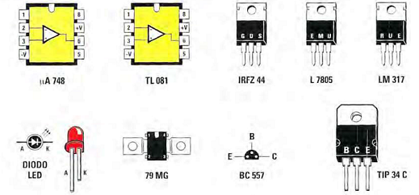
In figure 7 below, we have grouped the connections of the components used in the power supply. The connections of the uA748 and TL0B1 chips are seen from above, while those of the integrated stabilizers L7805 and LM317 are seen from the frontally. The connections of the MOSFET IRFZ44 and the transistor TlP34C are also seen from the frontally. The connections of the PNP transistor BC557 are instead seen from below. The integrated 79MG is designed with the connections seen from above. The Anode terminal of the LED is easily recognizable because it is longer than the Katodo terminal.
Figure 7
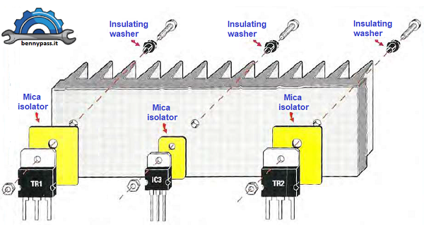
Transistor cooling system Figure. 8 below shows that the cooling fin has holes prepared to mount the two transistors PNP TIP34C (see TR1-TR2) and the integrated LM317 (voltage stabilizer, see IC3). All metal parts, from the bodies of the components to the screws with nuts used to screw them, must be electrically separated from the fin with insulating micas and washers.
Figure 8 The components
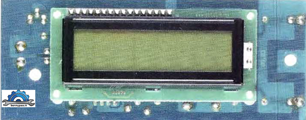
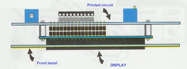
Display with Voltmeter and Ammeter
Figure 9 The display basically replaces what was once the analogue measurement like Figure 10 below
Figure 10
Figure 11 below shows the circuit diagram
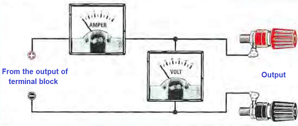
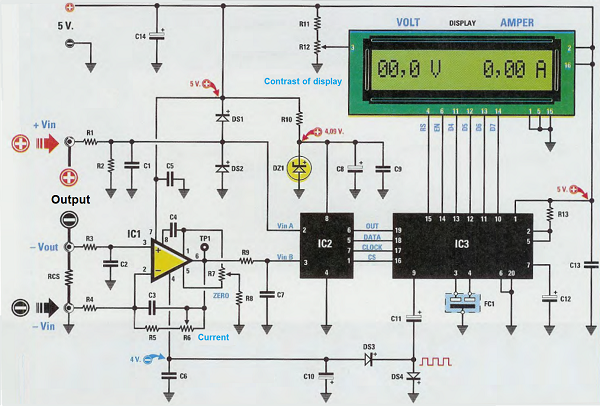
Figure 11 Figure 11 shows the Voltmeter and Ammeter wiring diagram. To energize the circuit needs a stabilized voltage of 5 volts, which you can take from our power supply as per details on the circuit board. To measure the volts supplied by the power supply, the positive voltage entering the resistive divider R1 - R2 will reach the VinA input of the double A/D converter marked lC2. Once transferred to the IC3 microprocessor, this will be displayed on the left side of the display. To measure the current absorbed by the circuit that we connect to the power supply, the negative voltage which entering to resistive part RCS - R3, will reach the inverting + input of the operational IC1, which will amplify the voltage drop by about 10 times which occurs on RCS resistance, then the amplified voltage will be applied to the Vin B input of the double-A / D converter labelled IC2. Once transferred to the IC3 microprocessor, this will be displayed on the right side of the display. Figure 12 below shows the RCS resistor
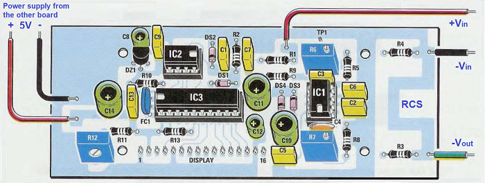
Figure12 As you can see from the practical diagram in fig. 12, the RCS resistor is a small U-shaped copper track that allows us to obtain the very low ohmic value that we would never be able to find on the market. To complete the description, we add that the IC3 microprocessor is a programmed ST62T10, which we also use to take a square wave frequency from pin 9, which will be rectified by the two diodes DS4-DS3, which allows us to obtain a negative voltage of approximately 4 volts which is used to power pin 4 of the operational amplifier IC1. The trimmers present in this circuit are used for:
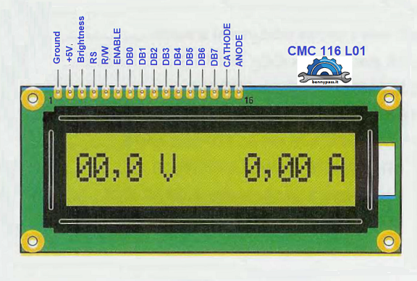
Components of the Display
Display installation
Figure 13 Before fixing the LCD on the printed circuit, you must perform a series of simple operations, as illustrated in the figures on these two pages.
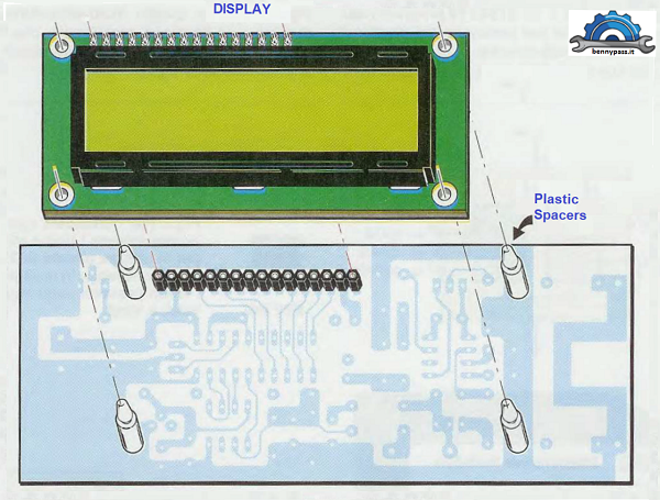
Figure 14 Fig 14. In the printed circuit, you have to insert the 16-hole female strip connector and the four plastic spacers to keep the display locked.
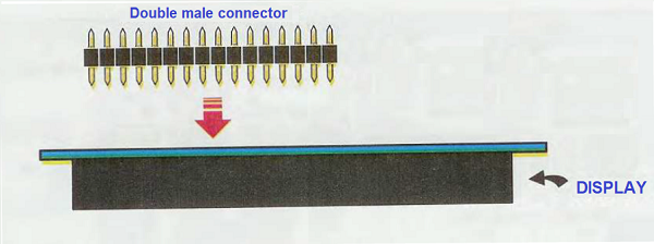
Fig. 15. On the body of the CMCJ16 / L01 display, insert the double 16 terminal male strip connector by soldering it into the holes on the printed circuit.
Figure 16 Fig. 16. Insert the 16-hole female strip connector and the 4 plastic spacers to support the display into the printed circuit (see fig. 14).
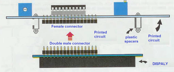
Figure 17 Fig. 17. After fixing the female connector in the printed circuit and the double male connector in the Display, you can plug it like in Figure 17
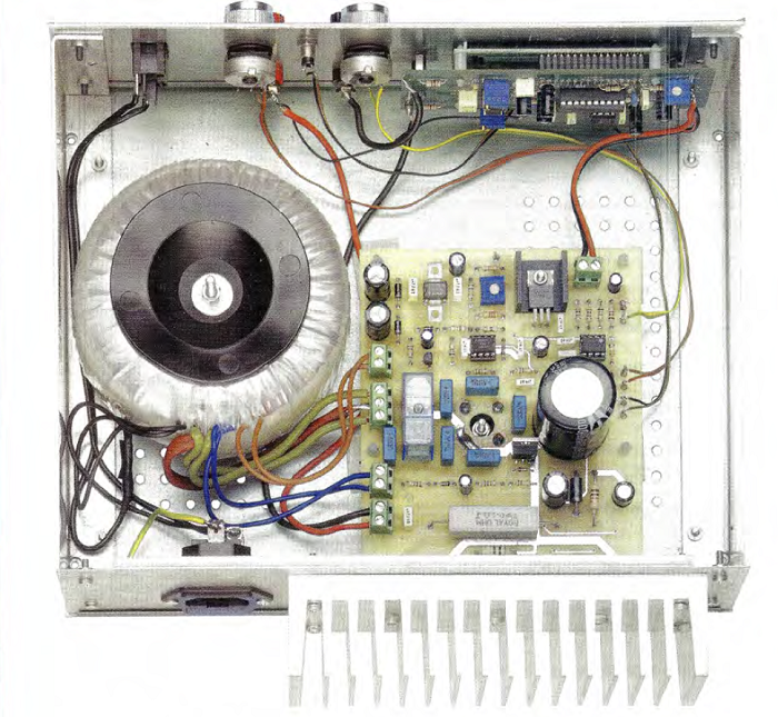
Conclusion A power supply design is not trivial because an efficient and professional tool must deliver the required current and provide the right voltage output without sitting down. It must be stable, and in the event of a fault in the powered appliance, it must be blocked. It must be protected from short circuits, warn the user of any problems, allow the technician time to remove the connections to discover the fault, and then power up the device again without any problem. He must be ready to carry out his work without uncertainty. Its internal characteristics allow the power supply to work without overheating the power amplifiers, thanks also to its internal relay that exchanges the voltage between (28 or 14Volts) according to the device's request (if it is lower than 12V or higher than 12Volt). There are mountains of power supplies on the market, maybe more beautiful even controlled by the microcontroller; in the end, it has nothing to do with it; what matters are the type of power amplifiers and their sensitivity to work and protection. For those who want to make this excellent power supply, printed circuits are available here on the website. The cost of components is 43 Euro + 23 euro for the casing with the cooling fins. The figure below shows the power supply assembled
Available also the display with PIC24 (microchip), which also include the controller.
www.bennypass.it |
|||||||||||||||||||


+(39) 347 051 5328
Italy - Kazakhstan


09.00am to 18.00pm
About
We offer the best and economical solutions, backed by 27+ years of experience and international standards knowledge, echnological changes, and industrial systems.
Our Services
Marketing Materials


Marketing Materials1


