A circuit board, also known as a printed circuit board (PCB), is a fundamental component in electronics. It’s the backbone of most electronic devices, providing a platform for the arrangement and interconnection of electronic components.
Circuit boards are found in nearly every electronic device, from simple devices like digital watches and calculators to complex devices like computers and televisions. They are designed to route electric signals through electronics, which allows the device to function as intended.
While circuit boards can be made manually via soldering techniques, professional circuit boards are made with printing technology, hence their name, Printed Circuit Boards (PCBs).
Since circuit boards allow electronic components to interact and work together, they enable the device's functionality. Without circuit boards, modern electronics as we know them would not exist.
Typically, circuit boards are made from an insulating material, often fibreglass (double or single-sided, or even multi-layered), and are coated with conductive materials. These conductive materials, usually copper, are etched to form pathways that electric currents can follow. These pathways, known as traces, connect the various components on the board, such as resistors, capacitors, and transistors, allowing them to work together to perform complex tasks.
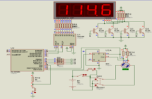
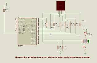
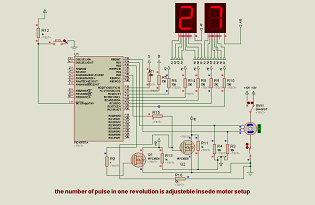
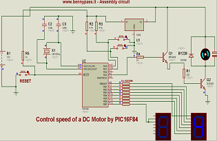
So, a circuit board combines semiconductors, insulators, and conducting materials to achieve a specific objective. i complessi. Figure below shows different types of circuit boards
|
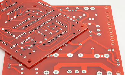 Figure 1- Single Sided PCB Figure 1- Single Sided PCB
|
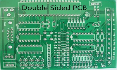 Figure 2- Double Sided PCB Figure 2- Double Sided PCB
|
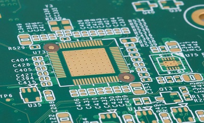 Figure 3 - Multilayer PCB Figure 3 - Multilayer PCB
|
There are many special features that are designed into the printed circuit board (PCB) that will increase the number of processing steps that it takes to complete the order. The combination of features can add additional cost to the raw PCB and increase the lead time to process.
When considering a PCB design and layout or redesign, it would be advantageous to consult with experts. Your printed circuit board supplier should have engineering resources to consult and review preliminary information and be able to assist with design suggestions.
Why High-Tech Multi-Layer PCB Features Add Cost and Processing Time
In this webinar we discuss multilayer features for printed circuit boards that add cost and processing time. We will also look at base costing materials, copper weights, common cost adders, plating finishes, processing, less common features, and more.


